About this Post
Transistors are often used as switches in the world of microcontrollers. MOSFETs are often chosen, especially when high currents need to be controlled. In principle, MOSFETs are very easy to handle, but there are still a few things to consider when working with them. In particular, the question arises as to which parameters you need to pay attention to in order to select the right MOSFET. Another question is which additional components are required. Do I need a series resistor at the gate? Do I need a gate driver? This article is intended to help answer these questions.
These are the topics I will discuss:
- What is a MOSFET?
- Minimum circuit
- Selection criteria
- Further considerations
- Gate driver
- Which MOSFET should I use?
What is a MOSFET?
You can find many articles online explaining the structure and operating principle of MOSFETs, e.g. here on Wikipedia. I will therefore only go into the essentials here.
The term MOSFET stands for Metal-Oxide Semiconductor Field-Effect Transistor. The MOSFET has three connections, which are called gate, drain and source. The voltage between the gate and source controls the current flow between the source and drain. Normally, the gate is on the left, drain in the middle and source on the right when you look at the labeled side of the MOSFET.
There are n-channel and p-channel MOSFETs. The n-channel MOSFET opens when the potential at its gate in relation to its source exceeds a certain positive threshold value. To open the p-channel MOSFET, on the other hand, a voltage must be applied to its gate that is negative in relation to the source. You use the n-channel MOSFET on the GND side and the p-channel MOSFET on the positive side of the supply voltage.

I will concentrate on the n-channel MOSFETs in my article.
MOSFET vs bipolar transistor
When we talk about a transistor, we usually mean a bipolar junction transistor (BJT). However, as MOSFETs also belong to the large family of transistors, I have to distinguish between them by name here.
Like MOSFETs, BJTs have three connections. And here too, the current flow between two of the connections, namely the collector and emitter, is controlled via the third connection, the base. However, they differ (among other things) in these aspects:
- In the BJT, a current flows from the base to the emitter. This controls the current flow from the collector to the emitter. The bipolar transistor is therefore current-controlled. In contrast, the MOSFET is voltage-controlled.
- The switching speed of the MOSFETs is higher than that of the BJTs.
- MOSFETs are more expensive.
- MOSFETs are suitable for higher currents.
- The BJT starts to conduct from a base-emitter voltage of around 0.7 volts. MOSFETs, on the other hand, generally require gate-source voltages of 1 to 4 volts.
- The MOSFET has a not inconsiderable parasitic capacitance. More on that later.
Minimum circuit
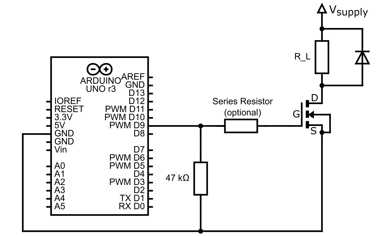
Let’s assume you want to switch a component that is operated with 5 volts. Furthermore, it needs a current that exceeds the limit of an I/O pin. This would be 20 mA for the Arduino UNO R3, for example. On the other hand, the current should only be high enough to be supplied via the 5 volt output of the microcontroller board. For USB operation, this is usually 500 milliamperes, minus 50 milliamperes for the board and minus what the I/O pins provide in total. In this case, the circuit can be designed very simply:

The load resistor R_L represents the device that you want to switch. I will go into the question of whether you need a series resistor. In most cases, you will be able to leave it out.
I tried out the circuit with an IRL520 MOSFET. One of the loads used was a 0.2 Watt LED (40 mA).
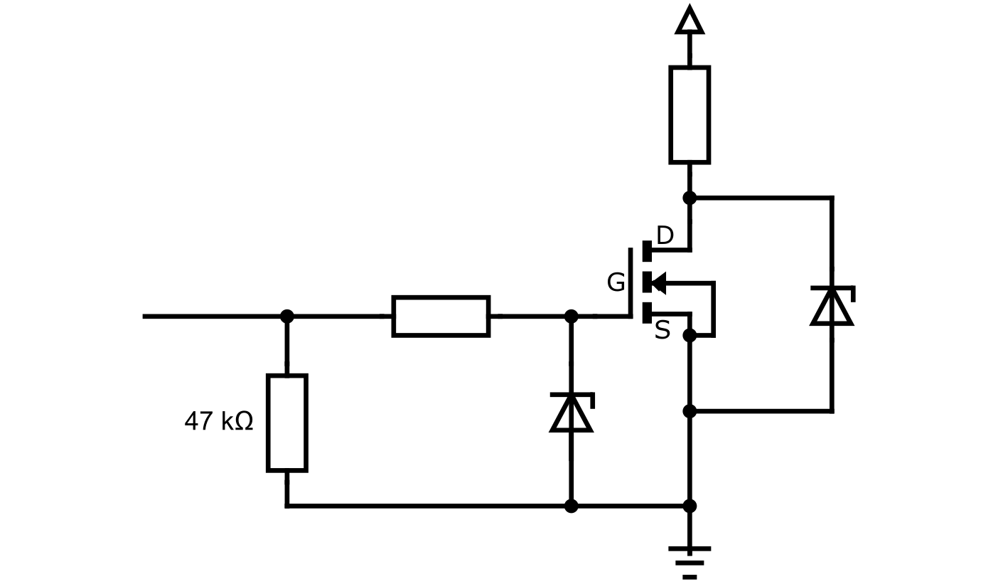
For the MOSFET to block reliably, it must be pulled to GND level. This is possible with the above circuit if pin 9 is set to OUTPUT/LOW. The safer option is to use an additional pull-down resistor (47 kΩ).
For higher current requirements or higher voltages, you must supply the load with a separate power source. If you are using a load that has a coil, such as a motor or an electromagnet, please keep in mind the obligatory freewheeling diode.
Selection criteria for MOSFETs
There is a huge range of MOSFETs available, which does not make the choice any easier. In addition, the data sheets are quite confusing for non-electronics engineers, as the list of specified properties is long. I will discuss the most important criteria below.
Logic Level MOSFETs
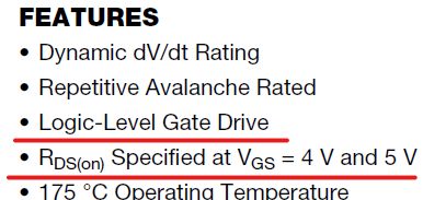
If you want to control a MOSFET with a gate-source voltage of 5 or even 3.3 volts, then you should use a logic level MOSFET. The first page of the data sheet usually states whether this is the case, as in the example on the right. In addition, the RDSON value (explanation follows) for the logic level MOSFETs is specified at 5 volts or lower and not, as is usually the case, at 10 volts. Another indicator is a low “Gate-Source Threshold Voltage”. This is the minimum gate-source (GS) voltage at which the MOSFET begins to conduct.

With logic level MOSFETs, the value is often between 1 and 2 volts; otherwise it is more likely to be 2 to 4 volts.
Many MOSFETs have a designation according to the scheme “IRFxxx” or “IRLxxx”. With “IRLs”, you can generally assume that it is a logic-level MOSFET. However, it is not certain that an “IRF” is not a logic-level MOSFET. You can find more abbreviations here on Mikrocontroller.net.
Maximum drain current
The data sheets of the MOSFETs specify the maximum drain current ID, as here for the IRL520:

However, the maximum ID depends on the gate-source voltage. You will find diagrams such as the following in the data sheets:
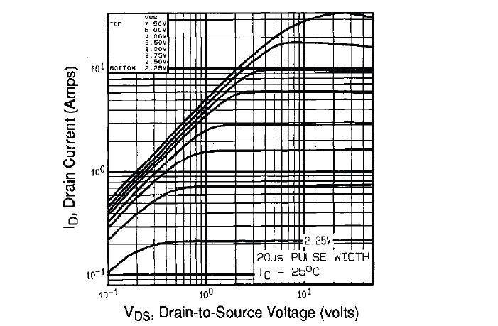

This is not as complicated as it may seem. Each of the curves indicates for a specific gate-source voltage how the current ID changes with the voltage between drain and source. The point is: For each gate-source voltage, there is a saturation range for ID. Perhaps this makes it even easier to understand: You have set a certain gate-source voltage in the circuit on the right, at which MOSFET conducts. Now you continuously increase the voltage Uvar. ID increases and with it the voltage drop across the load and across the drain source. If ID finally reaches the saturation range, the voltage drop across the load remains constant (U = R ⋅ I) and any additional increase in Uvar drops across the drain source without the current increasing any further.
Drain-source on resistance RDSON
Another important selection criterion is the drain-source restistance RDS(on). This is the resistance that drops across drain to source in the open state (“on”). An ideal switch has an infinitely high resistance when it is off and a resistance of zero when it is on. In this respect, the MOSFET is not a switch at all, but a controllable resistor! RDS(On) is comparatively small, but not negligible (again for the IRL520):

It should also be mentioned that RDS(On) is not constant, but increases as the gate-source voltage decreases.
At high currents, RDS(On) becomes noticeable through power losses, i.e. the transistor gets hot. Here is a small calculation: The gate-source voltage on an IRL520 is 5 volts. RDS(On) is therefore 0.27 Ohm. The current is 5 amperes. The power loss is therefore
![\[ P = U_\text{DS}[\text{V}]\cdot I_\text{D}[\text{A}]\; = R_\text{DS(On)}\cdot I_\text{D}\cdot I_\text{D} = 0.27\cdot 5 \cdot 5 = 6.75[\text{W]} \]](https://wolles-elektronikkiste.de/wp-content/ql-cache/quicklatex.com-65e8a3b2e4cd6cfd117c8840da23926c_l3.png "Rendered by QuickLaTeX.com")
To make matters worse, RDS(On) increases with the temperature:
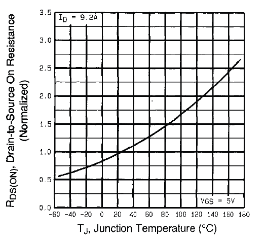
This easily doubles the power loss or even more.
The RDS(On) value of the IRL520 is quite high at 270 mΩ. There are MOSFETs with significantly lower resistances. The IRLB3034PbF, for example, is at the lower end with a maximum of 1.7 mΩ at a gate-source voltage of 4.5 volts. The power loss is correspondingly lower.
Further considerations
Do I need a heat sink?
Due to the potentially high power losses, the question arises whether you need to attach a heat sink to the MOSFET. To check this, look for the value for RθJA (Thermal Resistance Junction-To-Ambient) in the data sheet:

In this case (IRL520), the temperature increases by 62 degrees per watt. With the 6.75 watts calculated in the example above, you would initiate a catastrophic meltdown!
In the data sheets, you will find the maximum permissible temperature TJ (J = junction) for the MOSFET. A typical value is 175 °C. With the maximum expected ambient temperatureTA, this results in the maximum permissible power loss:
![\[ P_\text{max}=\frac{T_J-T_A}{R_{\Theta J\!A}} \]](https://wolles-elektronikkiste.de/wp-content/ql-cache/quicklatex.com-b0ab3c5406cf9362d38cd4d45fc33e8c_l3.png "Rendered by QuickLaTeX.com")
As already mentioned, the temperature dependency of RDS(On) must also be considered when calculating the power loss. If you install your circuit in an enclosure, the ambient temperature will also increase. In addition, you should not work permanently at TJ, but stay at least 30° below it.
These are all just estimates. You are responsible for your circuits – I accept no liability!
Do I need a series resistor at the gate?
In some circuits you can see resistors in front of the gate of the MOSFET, in other circuits not. Do you need them? I have found many controversial discussions about this on Microcontroller.net, e.g. this one here (very entertaining!). There are two aspects to this: One is unwanted electrical oscillations that can be caused by a fast charging of the gate, the other is the protection of the microcontroller. To anticipate, my conclusion is: as long as you are not working with very high PWM frequencies in combination with high gate capacitances, you can omit the series resistor. But one by one.
Base versus gate resistor
First of all, I would like to come back to the difference between the gate of a MOSFET and the base of a BJT. The base resistance for the BJT is essential, as only ~0.7 volts drop between the base and the emitter. Higher voltages lead to practically unrestrained currents.
The MOSFET, on the other hand, is voltage-controlled. No current flows from gate to source. However, the gate has a certain capacitance and therefore behaves like a capacitor. And to charge this capacitor, a time-limited current flows.
Experiments on gate resistance
I carried out a few experiments for this purpose. The starting point was this simple circuit:
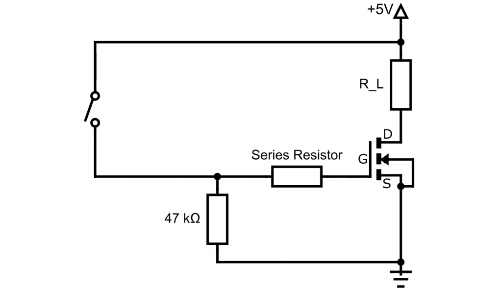
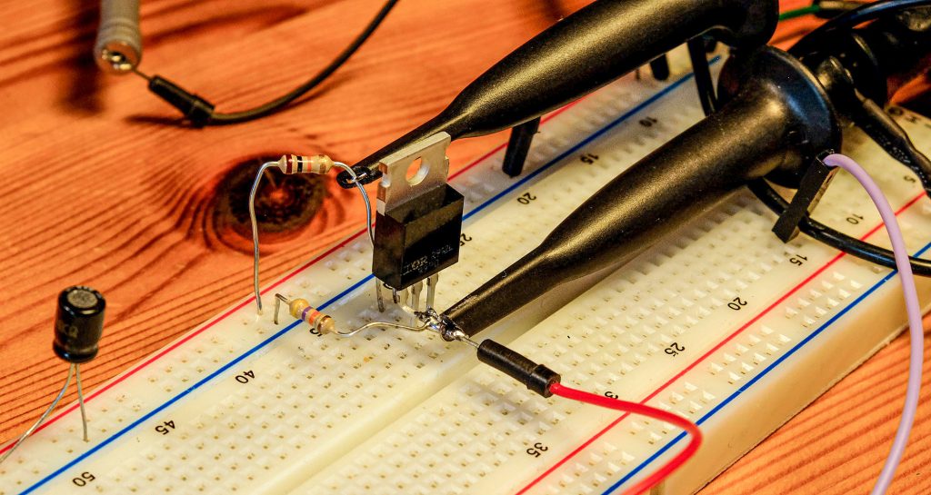
The IRL520 was again used as the MOSFET. The 5 volts were provided by a laboratory power supply. A 10 kΩ resistor was used as the load, i.e. a very low load. A pull-down resistor is required for this circuit; otherwise the gate would have an undefined potential. I soldered the resistor to the gate, as contacts on the breadboard produced noticeable resistances. I used the oscilloscope to monitor the gate-source and drain-source voltage.
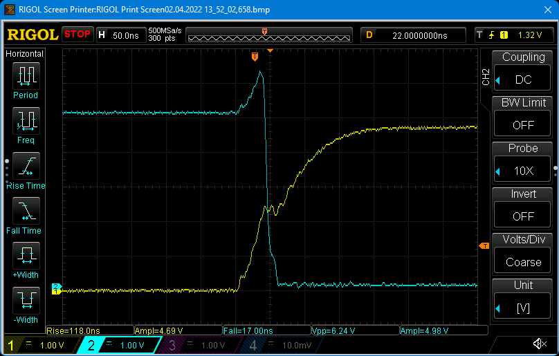
This is what the result looked like without a series resistor:

It took approx. 40 nanoseconds for the gate-source voltage to reach the applied voltage. The drain-source voltage drops to ID x RDS(On) in less than 3.6 nanoseconds once the “Gate-Source Threshold Voltage” is reached.
Now, there is another relevant specification in the data sheet, namely the “Total Gate Charge”. This is the maximum charge that must flow into the gate to fully charge it. I don’t have the conditions specified in the data sheet, but I just want to make a rough calculation.

This means that up to 12 nanocoulombs flow in approx. 40 nanoseconds. Current is charge per time, so the result is the current:
![\[ I=\frac{12\;[\text{nC}]}{40\;[\text{ns}]}=0.3\;[\text{A}]=300\;[\text{mA}] \]](https://wolles-elektronikkiste.de/wp-content/ql-cache/quicklatex.com-da95ba075a5b3354df79eeff4a4b2928_l3.png "Rendered by QuickLaTeX.com")
For the Arduino UNO, a limit of 20 milliamps is specified for the I/O pins. In the ATmega328P data sheet, the absolute maximum is specified as 40 milliamps. With the 300 mA, we are therefore far beyond this limit.
In another experiment, I connected the MOSFET to an Arduino I/O pin. To do this, I soldered the connection cable directly to the Arduino pin to keep resistances as low as possible:
In this case, charging the gate takes 120 nanoseconds.The Arduino pin cannot supply the required amount of charge as quickly as my laboratory power supply. The calculated current is 100 mA, which is still well above the specification.
Will I destroy my Arduino eventually? The prevailing opinion is no. If the load is in the nanosecond range, the Arduino can cope with it.
What happens with PWM?
With pulse width modulation, the microcontroller pin must load the gate at the PWM frequency. The analogWrite() function provides a PWM signal whose frequency depends on the board and the pin. For the Arduino boards, the frequency is ≤ 1000 Hz. At 1000 Hz, the average current would be (still related to the IRL520):
![\[ I = \frac{12 \cdot 1000\;[\text{nC}]}{1\;[\text{s}]}=12\;[\text{µA}] \]](https://wolles-elektronikkiste.de/wp-content/ql-cache/quicklatex.com-aa7fa4f9f6b6c3d77040fd34d341460a_l3.png "Rendered by QuickLaTeX.com")
That’s not a problem either:
However, if you need faster PWM frequencies, it can become problematic at some point. At some point, you will actually reach the specification limits for the continuous current. At 1000 kHz, the current is already 12 mA. And finally, there are also MOSFETs with significantly higher gate capacitances. In such cases, you can then use a MOSFET driver. But we will come to that later.
What does a series resistor do?
If you place a resistor in front of a capacitor, it will charge correspondingly more slowly. I have tested this with a 100 Ω and a 1 kΩ resistor in front of the gate:


The 100 Ω resistor increases the charging time of the gate from 40 to approx. 440 nanoseconds. The current to be supplied is correspondingly lower and the signals are cleaner. With the 1 kΩ resistor, the charging time is already approx. 3.6 microseconds.
Why Z-diodes?
In many MOSFET circuits you can see Z-diodes between gate and source and/or between drain and source. What is the benefit?
A Z-diode acts like a normal diode in the forward direction. In the reverse direction, it blocks up to its breakdown voltage and then becomes a good conductor. A Z-diode is therefore a kind of pressure relief valve, but for voltages. They are available with a wide range of different breakdown voltages. Incidentally, “Z-diode” is the generic term for Zener and avalanche diodes. The terms are often confused. Details can be found here, for example.
MOSFETs react allergically to overvoltages at the gate. They can be destroyed relatively easily as a result. Z-diodes are therefore well suited to protect the MOSFET or to avoid voltage peaks at the drain. The breakdown voltages must, of course, be adapted to the requirements of the MOSFET (e.g. maximum gate-source voltage) and the circuit (e.g. maximum expected drain-source voltage).
Here, for example, I have used a 5.1 volt Z diode for switching a 5 volt voltage in order to reduce the voltage peak between drain and source when the MOSFET opens:

So do you need Z diodes? Frankly, I don’t know how often MOSFETs actually die of overvoltage. But especially for complex projects with inaccessible circuits, you might want to think about it.
Gate driver
As you have seen, there can be problems with high PWM frequencies if the gate of the MOSFET is controlled via the I/O pin of a microcontroller. In addition, many MOSFETs still have a high RDS(On) value at gate-source voltages of 5 or even 3.3 volts and therefore a correspondingly high power loss.
Gate drivers (MOSFET drivers) are used to eliminate these problems. You can create these yourself with just a few components, or you can use gate driver ICs.
Gate driver circuits
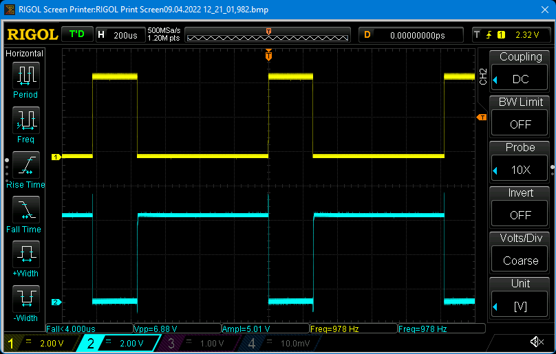
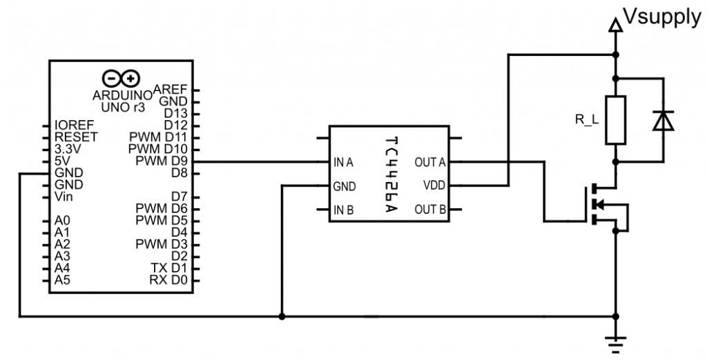
In the simplest case, you build a gate driver from a bipolar NPN transistor and two resistors. I used the following circuit to control a 12 V / 0.3 A electromagnet. The IRL520 was again used as the MOSFET and a BC547B as the transistor.

The MOSFET is open as the transistor is closed. This means that the magnet is active as long as pin 9 is LOW. If the magnet is to be switched off, pin 9 must be switched to HIGH. In the open state, a base-emitter and a collector-emitter current flow through the transistor. Base and collector resistance should not be selected too low from this point of view.
In this circuit, the MOSFET gate is controlled with the 5 volts of the Arduino. I could also have used the 12-volt power supply of my load. But then the IRL520 would no longer have been suitable, as its maximum gate-source voltage is 10 volts according to the data sheet.
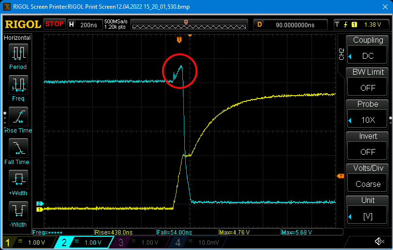
However, the gate’s loading time of 36.6 microseconds proves to be surprisingly slow, at least at first glance:
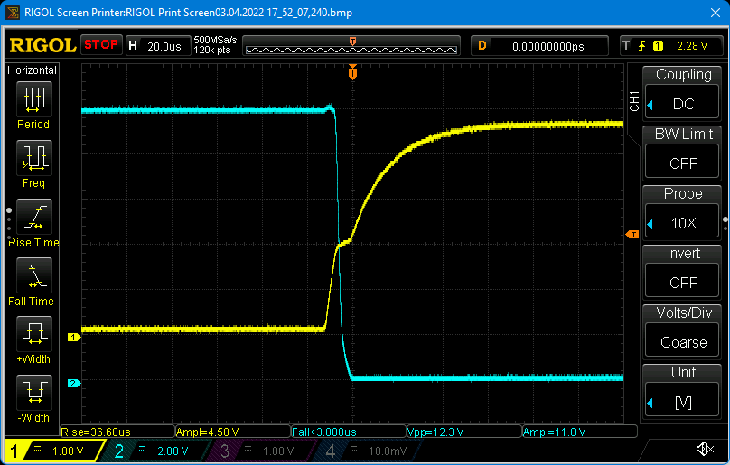
The explanation is that the gate is now charged via the 10 kΩ collector resistor. With a smaller resistor, it is proportionally faster, but at the price of a higher current flow. In addition to a smaller collector resistor, you can also choose a MOSFET with a lower capacitance. In the data sheet you will find the value “Input Capacitance”, i.e. the input capacitance.
Discharging the gate, on the other hand, is a very fast process (approx. 160 ns), provided you do not use a gate resistor. The speed-determining step is the switching of the transistor. Here too, the series resistor and the capacitance of the base form an RC element. It is faster with a smaller series resistor (84 ns at 1 kΩ).
With a PNP transistor as a gate driver, the reverse is true. Charging the gate is fast, discharging is slow.

Push-pull driver
With a push-pull driver circuit, you can both charge and discharge the gate quickly. It is a combination of an NPN and a PNP transistor. As one of the transistors is always closed, you do not need any resistors to limit the current on the driver side. Here is the simplest version:

If D9 is HIGH, the PNP transistor is closed, NPN is open, and the MOSFET gate is positive; hence, the magnet is active. You can also swap the NPN and PNP transistors to reverse the logic. However, you’ll need two separate base resistors for the transistors. You can find instructions on how to further customize the circuit and discover additional gate driver circuits here.
Gate driver ICs
Alternatively, you can buy gate driver ICs as ready-made solutions, such as the TC4426A or the IR2117. Using the TC4426A as an example, I will show you how to use such ICs.
Pinout TC4426A
You can control two MOSFETs with the TC4426A. It has the following inputs/outputs:

- NC: Not Connected
- IN A / IN B: Logic level input, HIGH signal: > 2.4 Volt
- GND / VDD: Power supply 4.5 – 18 volts
- OUT A / OUT B: Inverted output with voltage 0 V / VDD
Example circuit TC4426A
The wiring is very simple:
Limited suitability: MOSFET “driver modules”
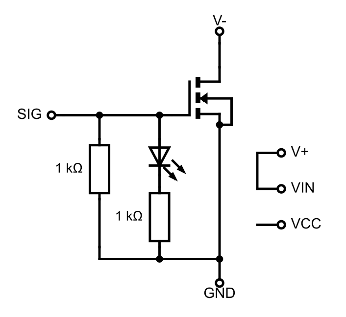
If you search for MOSFET drivers on Amazon and similar online stores, you will come across a so-called MOSFET driver module (see below). This name is misleading because this module does not drive anything! The signal input is connected directly to the gate of the MOSFET. The pull-down resistor is quite small at 1 kΩ. The MOSFET is an IRF520, i.e. not a true logic-level MOSFET. In addition, the connection designations are somewhat confusing, as three connections are not used at all. To the modules’ credit, I have to say that they work reliably with a signal voltage of 5 volts and that they indicate with the LED when a signal is present. The screw terminal connections can also be quite practical.

Which MOSFET should I use?
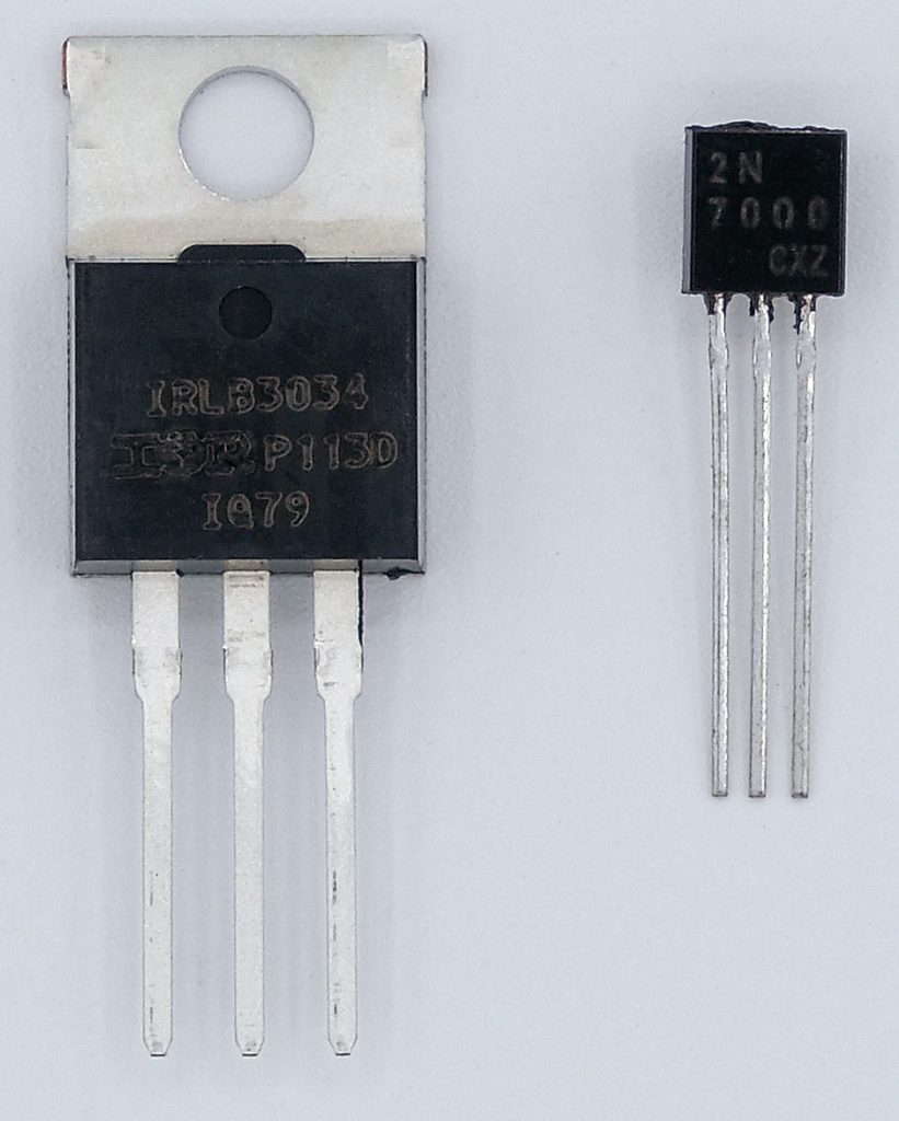
I hope this article will make you agree that the answer is: it depends! If you want to avoid the use of gate drivers, then go for a logic-level MOSFET first and foremost. For smaller currents, I would go for the smaller MOSFETs in TO-92 design such as the BS170 or the 2N7000. If large currents are to be controlled, the RDS(ON) should be small. The IRL3803, for example, is quite good in this respect. But these are just a few examples. You can find a very good overview of MOSFETs here at Mikrocontroller.net.
Acknowledgement
I have Joseph V M on Pixabay to thank for the switches in the picture.
Support requested
Did you enjoy this post? And did you notice that it’s ad-free? If you’d like to help keep it that way, follow this link.
Thanks
Helped a lot!
An amazing discussion
Thank you!