About this Post
In my article Using megaTinyCore I showed how to upload sketches to the ATtiny microcontrollers of the tinyAVR ® series 0, 1 and 2 using the board package from Spence Konde. In the next two posts, I will go into programming at register level. This will be relevant if, for example, you want to use the timers of the tinyAVR microcontrollers or special functions such as the Event System or the Configurable Customer Logic (CCL).
I have already given an overview of the tinyAVR family and its technical features here.
The data sheets of the tinyAVR microcontrollers have several hundred pages. Of course, I can’t cover all of that in this article. I won’t cover functions that you can also conveniently control via the Arduino language (Wire, SPI, etc.). But I also had to limit myself thematically. So it’s definitely worth taking a look at the data sheet!
Here’s what you can expect in this post and its sequels:
- Register programming of the tinyAVR series
- I/O Control – PORTx Module
- Reassigning Inputs / Outputs – PORTMUX Module
- The Event System – EVSYS Module
- Real-Time Counter – RTC Module
- Watchdog Timer – WDT Module
- A/D Converter – ADCn Module
- Timer A – TCAn Module (Part 2)
- Timer B – TCBn Module (Part 2)
- Configurable Custom Logic – CCL Module (Part 2)
- The tinyAVR MCUs go to sleep – SLPCTRL Module (Part 2)
- Timer D – TCDn Module (Part 3)
Serial output
And one more note in advance: in some sketches, I use Serial.print(). To get an output on the serial monitor, use a USB-to-TTL adapter and connect RX to TX, TX to RX and GND to GND. Don’t forget to set the port. If you are not uploading the sketches via UPDI, but already using the bootloader and USB-to-TTL adapter, then the serial output will work anyway.
Register programming of the tinyAVR series
I will now try to explain the basic principles of register programming for the tinyAVR series briefly. For detailed information, please refer to the application note TB3262 from Microchip.
Everything is a little different
The following blink sketch for pin PA2 gives a first impression:
void setup() {
    PORTA.DIRSET = PIN2_bm; // set PA2 (selectively!) to OUTPUT
}

void loop() {
    PORTA.OUTSET = PIN2_bm;  // set PA2 to HIGH
    delay(200);
    PORTA.OUTCLR = PIN2_bm;  // set PA2 to LOW
    delay(200);
}
This is very different from coding à la PORTA |= (1<<PA2) that you are probably more familiar with.
Register
The registers are organized in modules. The modules are structures (data type struct), which is why you can see the dot notation in the blink sketch. The name of the structure is the module, the registers are elements of this structure, e.g.
- PORTA.DIRSET:
- Module: PORTA
- Register: DIRSET
Bit Masks and Bit Group Configuration Masks
To understand bit masks and bit group configuration masks, let’s take a look at the Control A Register (CTRLA) of timer B0 as an example. The module is called TCB. However, as some tinyAVR microcontrollers have two timers B (0 and 1), the number is appended to the module name. In general terms: “MODULNAMEn.REGISTERNAME”. The CTRLA register of timer B0 is therefore called: TCB0.CTRLA.
The TCBn.CTRLA registers have various bits and the CLKSEL (Clock Select) bit group:

Bit masks are used to set single bits. Their names are formed according to the following scheme:
- MODUL_BIT_bm
The module number is omitted from the bit mask. This is, for example, how you set the ENABLE bit for the timer B0:
TCB0.CTRLA |= TCB_ENABLE_bm;
The bit group configuration masks are used for bit groups (also known as bit fields), the names of which are formed as follows:
- MODUL_BITGRUPPE_CONFIGURATION_gc
As an example, we specify that timer B0 uses the TCA clock:
TCB0.CTRLA |= TCB_CLKSEL_TCA0_gc;
CLKTCA corresponds to the CLKSEL value 0x2 or 0b10. In the register, CLKSEL is located at bit position 1 and 2, i.e. it is shifted 1 bit to the left. This is why the value of TCB_CLKSEL_TCA0_gc is 0x4 or 0b100.
If you want to mask the bit group TCB_CLKSEL, you can use the bit group mask. Here in the general form:
- MODUL_BITGRUPPE_gm
The value of TCB_CLKSEL_gm is 0x6 or 0b110, as you can easily check with Serial.println(TCB_CLKSEL_gm, BIN).
Bit Positions and Bit Group Positions
Then there are the Bit Positions and the Bit Group Positions:
- MODUL_BIT_bp
- MODUL_BITGRUPPE_gp
Unsurprisingly, they indicate the position of the bit or bit group in the register. So if you want to determine the current CLKSEL value of timer TCB0, you could do it like this:
Serial.println( ((TCB0.CTRLA & TCB_CLKSEL_gm) >> TCB_CLKSEL_gp) );
It may all sound a little complicated at first, but you soon get used to this type of notation. It involves a certain amount of writing, but it pays off because the code is still easy to understand even after a few months.
Orientation in the Data Sheet
This way of programming registers takes some getting used to at first. What helps with orientation is the data sheet of the tinyAVR MCU in question. It is organized according to the modules and for each module there is a “Register Summary” with links to the individual registers, where you can then find the bit masks and bit group masks.

I also recommend looking at the “I/O Multiplexing and Considerations” section of the data sheet. There you will find a table showing which pins have which functions.
Looking up the definitions
Sometimes (but rather rarely) the names for the bitmasks, bitgroups etc. in the data sheet are inconsistent with the names you have to use in the program. Fortunately, the compiler usually provides you with the correct alternative.
Otherwise, you will find the definitions in the Arduino installation. Where exactly depends on your installation. For me, the directory is under:
C:\Users\Ewald\AppData\Local\Arduino15\packages\arduino\tools\avr-gcc\7.3.0-atmel3.6.1-arduino5\avr\include\avr
The files for the ATtinys have the designation iotnxxx.h. But even if you don’t have a problem, it is worth taking a look at this.
I/O Control – PORTx Module
PORTx Register
DIR, OUT and IN registers
As demonstrated by the register summary above, there are a number of registers whose names begin with “DIR” or “OUT”. The “DIR …” registers control which pins are used as INPUT or OUTPUT. With the help of the “OUT …” registers you set the pin level, i.e. HIGH or LOW. The second part of the name means:
- SET: sets bits in OUT and DIR → OUTPUT or HIGH
- CLR: clears bits in OUT and DIR → INPUT or LOW
- TGL: toggles the status.
You can also write directly to the DIR and OUT registers, but the beauty of OUTSET, OUTCLR, OUTTGL and their DIR counterparts is that the instructions are pin-selective. Example:
PORTx.OUT = PINy_bm;sets pin y (with y = 0 to 7) of port x to HIGH and all other pins of port x to LOW. Here x = A, B or C, depending on which ports are available.PORTx.OUTSET = PINy_bm;only acts on pin y, i.e. the statement corresponds toPORTx.OUT |= PINy_bm;.
You can use the IN registers to read the status of the pins (digitalRead(), so to speak). However, if you write a bit to the PORTx.IN register, the corresponding bit is toggled in PORTx.OUT. The IN register is the counterpart to the PINx register of traditional AVR microcontrollers.
Control Register PINxCTRL
Each pin has its own control register, namely PINxCTRL:

The INVEN bit allows you to invert the INPUT and OUTPUT values. PULLUPEN activates the internal pull-up resistor. With ISC you can define the interrupt conditions or switch off the digital function of the pin completely (INPUT_DISABLE):
![ISC[2:0] Bit Group Configurations](https://wolles-elektronikkiste.de/wp-content/uploads/2023/11/PINxCTRL_ISC_table.webp)
Example Sketches for PORTx
Switching Pins
I’ll come back to the blink sketch and show that there are other ways to achieve the same effect:
void setup() {
    PORTA.DIRSET = PIN2_bm; // set PA2 to OUTPUT
    // PORTA.DIR |= (1<<2);
    // PORTA.DIR |= (1<<PIN2_bp); // bp = bit position
}

void loop() {
    PORTA.OUTSET = PIN2_bm;  // set PE2 to HIGH
    // PORTA.OUT |= PIN2_bm;
    delay(200);
    PORTA.OUTCLR = PIN2_bm;
    // PORTA.OUT &= ~PIN2_bm;
    delay(200);

    // Alternative: toggle pin:
    // PORTA.OUTTGL = PIN2_bm;
    // delay(200);
}
Reading Pin Levels
Here is an example of how you can read out individual pins. To do this, connect an LED to PA2 and a push-button, which emits a HIGH signal when pressed, to PA1. As long as you press the button, the LED lights up.
void setup() {
    PORTA.DIRSET = PIN2_bm; // PA1: OUTPUT
    PORTA.DIRCLR = PIN1_bm; // PA2: INPUT
}

void loop(){
    if(PORTA.IN & PIN1_bm){
        PORTA.OUTSET = PIN2_bm;
    }
    else{
        PORTA.OUTCLR = PIN2_bm;
    }
}
Setting up Interrupts
The following is a simple example of an interrupt on PA1. Apart from the button, which should provide a LOW signal when pressed this time, you use the setup of the last example. Note that the interrupt is not automatically cleared by calling the ISR. You must “manually” clear the bit in the relevant interrupt flag register.
volatile bool event = false;

ISR(PORTA_PORT_vect){
    PORTA.INTFLAGS = PIN1_bm; // clear interrupt (writing a "1" clears the bit!)
    event = true;
}

void setup() {
    PORTA.DIRSET = PIN2_bm;
    PORTA.DIRCLR = PIN1_bm;  // redundant in this case
    PORTA.PIN1CTRL = PORT_PULLUPEN_bm | PORT_ISC_BOTHEDGES_gc; // Pull-Up / Interrupt n both edges
}

void loop(){
    if(event){
        PORTA.OUTSET = PIN2_bm;
        delay(1000);
        PORTA.OUTCLR = PIN2_bm;
        event = false;
    }
}
An interrupt is triggered both when the button is pressed and when it is released. This is only really noticeable if the button is pressed for longer than one second.
Virtual Ports
If you use port manipulation à la PORTA.OUT = (1 << 2);, you should use the virtual port registers instead of the “normal” port registers. To do this, simply place a “V” before PORTx, i.e.: VPORTA.OUT = (1 << 2);. The virtual ports are copies of the ports in the lower address space. Port manipulations are performed faster when using the virtual ports. The following code took 501 milliseconds to execute on an ATtiny3226 at 20 MHz:
for(unsigned long i=0; i<1000000;i++){
    PORTA.OUT = 0;
    PORTA.OUT = (1<<2);
}
The same code, but with VPORTA.OUT instead of PORTA.OUT required 400 milliseconds. These are not major differences, but they are differences nonetheless.
The available VPORTx registers are DIR, OUT, IN and INTFLAGS.
Reassigning Inputs / Outputs – PORTMUX Module
The registers of the PORTMUX module allow you to assign certain functions to alternative pins. It is best to check the PORTMUX Register Summary to see which functions these are. Here, as an example, is the PORTMUX Register Summary of the ATtiny3224/6/7:

As an example, we redirect the output 1 of timer TCA0. The relevant PORTMUX register is TCAROUTEA. By setting the relevant bit, you change from the default to the alternative:
PORTMUX.TCAROUTEA |= PORTMUX_TCA01_bm;
The Event System – EVSYS Module
The event system is really cool! It allows certain peripherals, i.e. timers, ADC, USART, etc., to send signals to other peripheral units without involving the CPU. Later in the article, we will have the RTC timer regularly trigger ADC measurements. Normally, you would probably do this via delay(), millis() or timer interrupts. However, all these options have certain disadvantages.
3 or 6 channels are available for transmitting the event signals. The sender of the signal is called the generator, the receiver is the user. Many users have their own event control register in which further settings can be made. These registers are part of the peripheral modules.
Generators and users can be synchronous or asynchronous to the system clock. If an asynchronous generator sends an event signal to a synchronous user, the signal must first be synchronized, which takes a few clock cycles. For now, it is only important that you have heard of the distinction.
EVSYS module of the tinyAVR series 2
CHANNELn Register – Definition of the Generator
In the CHANNELn registers (with n = 0 to 5) you define the generator:

Most generators can utilise all channels. But there are also exceptions. For example, the pins of port A can only use channels 0 to 3. Here is a small excerpt from the ATtiny3224/6/7 data sheet:

Select a suitable channel and assign the generator to its register (EVSYS.CHANNELn). Compose the generator name according to the following recipe:
“EVSYS_” + “CHANNELn_” + Peripheral_ + Output_ + “gc”
For example: EVSYS_CHANNEL0_PORTA_PIN1_gc;
Register USERn – Definition of the users
You define the event users in the USERn registers:

Here is an excerpt from the table of available event users:

The complete table(s) can be found in the data sheet in the EVSYS chapter in the register descriptions. The names of the USER registers are composed as follows:
“EVSYS.USER” + “Peripheral” + “Input”
For example, EVSYS.USEREVSYSEVOUTA. You assign the channel to the USER register from which it is sent.
A simple event example
For a better understanding, let’s take a look at a small example (tested on ATtiny3226). Attach an LED to PA2 and a pushbutton, which pulls the pin LOW when pressed, to PA1.
Now we use PA1 as an event generator and EVOUTA (=PA2) as a user. Channels 0 to 3 are available for port A. In the example, we use Channel 0.
void setup() {
    PORTA.DIRCLR = PIN1_bm; // PA1 INPUT
    PORTC.DIRSET = PIN2_bm; // PA2 (=EVOUTA) OUTPUT
    PORTA.PIN1CTRL |= PORT_PULLUPEN_bm;

    EVSYS.CHANNEL0 = EVSYS_CHANNEL0_PORTA_PIN1_gc;  // PA1 is event generator for channel 0
    EVSYS.USEREVSYSEVOUTA = EVSYS_USER_CHANNEL0_gc;  // EVOUTA is user of event channel 0
}

void loop(){}
PA2, or EVOUTA, reflects the status of PA1. The LED lights up in the normal state and switches off when the button is pressed. This may not be impressive at first glance, but at second glance it is. We do not query the level of PA1, nor have we set up an external interrupt for it. In addition, there are no instructions for switching the LED in the running program. The processes are all controlled in the background without your running program having to do anything. More useful applications will follow later.
EVSYS of the tinyAVR series 0 and 1
The event system of tinyAVR series 0 and 1 differs from that of series 2. There are separate registers for the synchronous and asynchronous generators and users. However, the basic principle is the same, which is why I won’t go into detail here. Take a look at the data sheet yourself, search for the EVSYS chapter and perhaps go to the register summary first. This will give you an overview, and you can navigate to the registers from there.

EVSYS example sketch for tinyAVR series 0 and 1
To help you get started, here is an example sketch for the tinyAVR series 1 and 0. It basically does the same thing as the example for series 2. I tested the sketch on an ATtiny1604 and ATtiny1614.
void setup() {
    PORTA.DIRCLR = PIN1_bm; // PA1 INPUT
    PORTA.DIRSET = PIN2_bm; // PA2 (=EVOUT0) OUTPUT
    PORTA.PIN1CTRL |= PORT_PULLUPEN_bm;

    PORTMUX.CTRLA |= PORTMUX_EVOUT0_bm; // Event output needs to be enabled for tinyAVR 0/1
    EVSYS.ASYNCCH0 = EVSYS_ASYNCCH0_PORTA_PIN1_gc; // PA1 is async. event generator for channel 0
    EVSYS.ASYNCUSER8 = EVSYS_ASYNCUSER8_ASYNCCH0_gc;  // ASYNCUSER8 = EVOUT0 = channel 0 user
}

void loop(){}
In addition to the differences already mentioned, it is noticeable here that the “x” in the EVOUTx is a number and not a letter. It should also be noted that the event output (EVOUTx) must be activated in the PORTMUX.CTRLA register. Finally, it should also be mentioned that the SYNCUSER and ASYCUSER registers are not named by their user, but are numbered consecutively. The numbers can be found in the data sheet in the description of the (A)SYNCUSER registers.
Real-Time Counter – RTC Module
The RTC module has two features, namely the 16-bit Real-Time Counter (RTC) and the Periodic Interrupt Timer (PIT). Both use the same clock source. Otherwise, the functions can be used independently of each other. The maximum clock rate is 32768 Hz, so you are more likely to control the slower processes with this module.
The registers of the RTC module
Conveniently, the register landscape of the RTC module is almost identical for all tinyAVR representatives. There are differences in the calibration and the selection of clocks.
Clock Selection Register CLKSEL

The clock is set in the CLKSEL register. The following options are available:
- INT32K_gc: 32768 Hz provided by the internal ultra low-power oscillator OSCULP32K.
- INT1K_gc: Like INT32K, but with a divider of 32, i.e. 1024 Hz.
- TOSC32K_gc: 32768 Hz through XOSC32K or an external clock at TOSC1.
- only applies to tinyAVR series 1 and 2.
- EXTCLK_gc: External clock generator connected to EXTCLK.
Crystal Frequency Calibration Register CALIB (tinyAVR Series 2 only)
A really great feature of the series 2 RTC module is that you can calibrate the underlying clock using the CALIB register.

ERROR[6:0] is the deviation in ppm. If SIGN is set, the clock is correspondingly faster. In this case, you must set the prescaler to at least DIV2. If SIGN is not set, the clock is slower.
RTC Control Register A CTRLA
In the CTRLA register, you specify whether the RTC module should continue to run in standby mode (RUNSTDBY). You also (de)activate the calibration (CORREN, if available) and switch on the module (RTCEN).

You can use the PRESCALER to slow down the RTC with a maximum factor of 32768:
![PRESCALER[3:0] Bit Group Configurations](https://wolles-elektronikkiste.de/wp-content/uploads/2023/11/Reg_RTC_DIV_table-1024x381.webp)
RTC Interrupt Control Register INTCTRL
A Compare Match and an Overflow Interrupt are available for the RTC. The corresponding Interrupt Flag Register INTFLAG is similar.

There is only one interrupt vector, namely RTC_CNT_vector, i.e. you have to look in the INTFLAGS register to see which interrupt was triggered.
PIT Control Register A CTRLA
The Periodic Interrupt Timer simply does what its name suggests: It triggers an interrupt at regular intervals. In the PITCTRLA register, you can activate the PIT and set the period.

![PERIOD[3:0] Bit Group Configurations](https://wolles-elektronikkiste.de/wp-content/uploads/2023/11/Reg_RTC_CYCLE_table.webp)
PIT Interrupt Control Register PITINTCTRL
In PITINTCRTL you activate the PIT interrupt. PITINTFLAGS is similar to PITINTCTRL.

Example Sketches for RTC and PIT
RTC example sketch
As a simple example for programming the RTC, a sketch follows, which generates a “slow motion PWM” with a period of 2 seconds and a duty cycle of 75 % at PA2.
ISR(RTC_CNT_vect){
    if(RTC.INTFLAGS & RTC_CMP_bm){ // check for CMP interrupt
        RTC.INTFLAGS = RTC_CMP_bm; // delete CMP interrupt flag
        PORTA.OUTCLR = PIN2_bm; // PA2 = LOW
    }
    if(RTC.INTFLAGS & RTC_OVF_bm){ // check for OVF interrupt
        RTC.INTFLAGS = RTC_OVF_bm; // delete OVF interrupt flag
        PORTA.OUTSET = PIN2_bm;  // PA2 = HIGH
    }
}

void setup() {
    delay(1);
    PORTA.DIRSET = PIN2_bm;
    RTC.CLKSEL = RTC_CLKSEL_INT32K_gc; // set internal clock @ 32768 Hz
    RTC.PER = 16383;  // TOP = 16383
    RTC.CMP = 12288;  // Compare value = 12288
    RTC.INTCTRL = RTC_CMP_bm | RTC_OVF_bm;  // enable CMP and OVF interrupts
    RTC.CTRLA = RTC_PRESCALER_DIV4_gc | RTC_RTCEN_bm; // Prescaler = 4 and enable RTC
}

void loop(){}
As only one interrupt vector (RTC_CNT_vect) is available for the Overflow and Compare Interrupt, we have to use the interrupt flags to check which event triggered the interrupt.
The prescaler is set to 4, i.e. the RTC counts at a frequency of 32768 / 4 = 8192 Hz. PER is 16383 and therefore the RTC overflows every 16384 steps, which corresponds to an overflow frequency of 2 seconds. The Compare Value is 12288, i.e. 75% of PER +1.
PIT example sketch 1
The example sketch for the PIT is even simpler. With a period of 16384 and a clock rate of 32768 Hz, an interrupt is triggered every 0.5 seconds. We use it here to toggle PA2.
ISR(RTC_PIT_vect){
    RTC.PITINTFLAGS = RTC_PI_bm; // clear PIT interrupt flag
    PORTA.OUTTGL = PIN2_bm; // toggle PA2
}

void setup() {
    PORTA.DIRSET = PIN2_bm;
    RTC.CLKSEL = RTC_CLKSEL_INT32K_gc; // set internal clock @ 32768 Hz
    RTC.PITINTCTRL = RTC_PI_bm;  // enable PIT interrupt
    RTC.PITCTRLA = RTC_PERIOD_CYC16384_gc | RTC_PITEN_bm; // interrupt frq.: 2 Hz
}

void loop(){}
PIT example sketch 2
However, you can also achieve the same without an interrupt by using PIT as an event generator. The event signal has a duty cycle of 50%. Here is a version for an ATtiny1614:
void setup() {
    PORTA.DIRSET = PIN2_bm;
    RTC.CLKSEL = RTC_CLKSEL_INT1K_gc; // set internal clock @ 1.024 kHz
    RTC.PITCTRLA = RTC_PITEN_bm;
    PORTMUX.CTRLA |= PORTMUX_EVOUT0_bm; // Event output needs to be enabled for tinyAVR 0/1
    EVSYS.ASYNCCH3 = EVSYS_ASYNCCH3_PIT_DIV1024_gc; // Event freq. = 1024 / 1024 = 1 [Hz]
    EVSYS.ASYNCUSER8 = EVSYS_ASYNCUSER8_ASYNCCH3_gc;
}

void loop(){}
Watchdog Timer – WDT Module
The registers of the WDT Module
The watchdog timer behaves in the same way on all members of the tinyAVR family. I find two features particularly remarkable:
- The WDT does not have an interrupt vector.
- A WDT timeout always leads to a reset.
The Watchdog Timer (WDT) receives its clock from the ultra low-power oscillator, OSCULP32K.
Control A Register CTRLA
You enter the timing parameters for the WDT in control register A, CTRLA.

You can make the following settings for PERIOD and WINDOW:
![WINDOW[3:0] / PERIOD[3:0] Bit Group Configurations](https://wolles-elektronikkiste.de/wp-content/uploads/2023/11/wdt_ctrla_settings-1024x404.webp)
If you only set a value for PERIOD and keep WINDOW at 0, the WDT will run in Normal Mode. If no watchdog reset takes place within the time period defined with PERIOD, a system reset is carried out.
If WINDOW is not zero, you are in Window Mode. This is a little more difficult to explain, and perhaps only becomes clear with the example sketch. The following applies in window mode:
- After initialization or a
wdt_reset(), the WDT is in the period defined by WINDOW. The data sheet calls this period “closed window time-out period” (TOWDTW). The WDT cannot be reset during this period. Awdt_reset()within this period leads to an immediate system reset. - After the TOWDTW, the “normal window time-out period” (TOWDT) begins, the length of which you specify with PERIOD. If a
wdt_reset()is received during this time, the game starts again from the beginning with the TOWDTW. - If there is no
wdt_reset()in the TOWDTW + TOWDT period, a system reset is carried out.
Status Register STATUS

By setting the LOCK bit, you protect the WDT settings against changes. You can only delete it again in debug mode.
If you write data to the CTRLA register, it must be transferred to the WDT clock domain. The SYNCBUSY bit is set during synchronization.
Example Sketch for the WDT
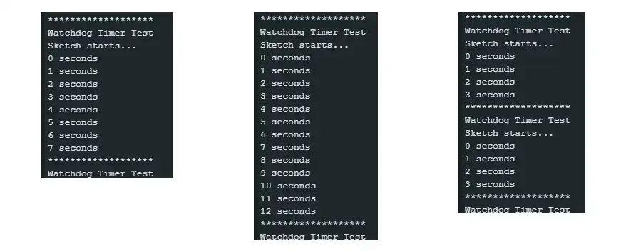
Normal mode should not require an example sketch. We will therefore only look at one sketch for window mode. The setting for the WDT is: TOWDTW = TOWDT = 4 seconds.
#include <avr/wdt.h>
void setup(){
    Serial.begin(115200);
    Serial.println("*******************");
    Serial.println("Watchdog Timer Test");
    Serial.println("Sketch starts...");
    CPU_CCP = CCP_IOREG_gc; // allow changes
    WDT.CTRLA = WDT_WINDOW_4KCLK_gc | WDT_PERIOD_4KCLK_gc; // 4s period and window
    CPU_CCP = CCP_IOREG_gc;
    WDT.STATUS = WDT_LOCK_bm;
    while(WDT.STATUS & WDT_SYNCBUSY_bm){} // wait until WDT is synchronized
    wdt_reset();
    int seconds = 0;
    while(seconds < 100){
        // if(seconds == 5){  // try also 3
        //     wdt_reset();
        // }
        Serial.print(seconds);
        Serial.println(" seconds");
        delay(1000);
        seconds++;
    }
}

void loop(){}
If you let the sketch run unchanged, the while() loop counts up until TOWDTW + TOWDT = 8 seconds have passed. The last output is “7 seconds” because once the eighth second has been reached, there is no more time for the output of “8 seconds”.
If you uncomment lines 15 to 17, there is a wdt_reset() at fifth second, i.e. in the “allowed” TOWDT period. The WDT then runs for a further eight seconds until the system reset is carried out.
If you then change line 15 so that the wdt_reset() occurs after three seconds, there will be an immediate system reset as you are in the “forbidden” TOWDTW period.
And what’s the point of all this? The watchdog normally bites if the sketch gets stuck somewhere. You can use the window method to trigger a system reset if an action is executed too early, for example because some other step has not been executed for whatever reason.
A/D Converter – ADCn Module
The A/D converter of the tinyAVR microcontroller would certainly deserve a separate article. However, I will keep this chapter short and once again refer to the data sheets.
The ADC modules of tinyAVR series 0 and 1 differ fundamentally from those of series 2.
ADCn of the tinyAVR series 0/1
Here is the identical register structure for all tinyAVR MCUs of series 0 and 1:

I would like to explain a few selected register settings:
- RUNSTBY: Allows the ADC to be operated in standby mode.
- RESSEL: If you set this bit, the resolution is reduced from 10 to 8 bits.
- FREERUN: Continuous mode.
- SAMPNUM: You can add up to 64 results per measurement. 2^6 results times 2^10 resolution gives a result with a size of 2^16 bits, which still fits into the RES result register.
- PRESC: Divider for the clock rate of the ADC.
- REFSEL: Selection of the reference voltage. The following options are available: INTREF (Internal Reference), VDDREF and VREFA (External Reference, not for ). Confusingly, the data sheet states “INTERNAL” and “VDD” instead of INTREF or VDDREF.
- SAMPLEN: Extends the measuring time up to a maximum factor of 31.
- MUXPOS: Defines the input for the ADC. The table with the bit group configurations can be found in the data sheet.
- STARTCONV: Starts a measurement.
The internal reference is specified in the VREF.CTRLA register. To do this, set the bit group ADC0REFSEL[2:0]. The Bit Group Configurations are called VREF_ADC0REFSEL_xxx_gc with
- xxx = 0V55, 1V1, 2V5V, 4V34 V or 1V5 for 0.55, 1.1, 2.5, 4.34 or 1.5 volts.
Example sketches for the ADC (tinyAVR series 0/1)
Simple A/D measurement (series 0/1)
In the following example sketch, we measure the voltage at A2. We use the internal 4.34 V reference voltage.
void setup() {
    Serial.begin(115200);
    PORTA.PIN2CTRL = PORT_ISC_INPUT_DISABLE_gc; // Disable digital buffer
    ADC0.CTRLA = ADC_ENABLE_bm; // Enable ADC
    ADC0.CTRLC = ADC_REFSEL_INTREF_gc | ADC_PRESC_DIV16_gc; // use internal reference / prescaler: 16
    VREF.CTRLA = VREF_ADC0REFSEL_4V34_gc; // use internal 4.34 V reference
    ADC0.MUXPOS = ADC_MUXPOS_AIN3_gc; // use A3 as input
    ADC0.SAMPCTRL = 0;
}

void loop(){
    ADC0.COMMAND = ADC_STCONV_bm; // Start Conversion
    while((ADC0.INTFLAGS & ADC_RESRDY_bm) == 0){} // Waiting for the result
    float result = ADC0.RES * 4340.0 / 1024.0;
    Serial.print("Voltage [mV]: ");
    Serial.println(result);
    delay(1000);
}
ADC0 – RTC controlled (Series 0/1)
Let me come back to the events. The following sketch uses the RTC to initiate an ADC conversion every two seconds.
volatile bool adcReady = false;

ISR(ADC0_RESRDY_vect){
    adcReady=true;
}

void setup() {
    Serial.begin(115200);
    PORTA.PIN3CTRL = PORT_ISC_INPUT_DISABLE_gc;
    ADC0.CTRLA = ADC_ENABLE_bm;
    ADC0.CTRLC = ADC_SAMPCAP_bm | ADC_REFSEL_INTREF_gc | ADC_PRESC_DIV16_gc;
    VREF.CTRLA = VREF_ADC0REFSEL_4V34_gc;
    ADC0.MUXPOS = ADC_MUXPOS_AIN3_gc; // A3
    ADC0.SAMPCTRL = 0;
    ADC0.EVCTRL = ADC_STARTEI_bm; // initiate measurement by event
    ADC0.INTCTRL = ADC_RESRDY_bm; // enable result ready interrupt
    RTC.CLKSEL |= RTC_CLKSEL_INT32K_gc; // use internal 32 kHz clock
    RTC.PER = 63; // overflow after 63 (64 steps)
    RTC.CTRLA = RTC_PRESCALER_DIV1024_gc | RTC_RTCEN_bm; // OVF frequency = 0.5 Hz

    EVSYS.ASYNCCH0 = EVSYS_ASYNCCH0_RTC_OVF_gc; // RTC overflow is event generator
    EVSYS.ASYNCUSER1 = EVSYS_ASYNCUSER1_ASYNCCH0_gc; // ADC0 is event user
}

void loop(){
    if(adcReady){
        float result = ADC0.RES * 4340.0 / 1024.0;
        Serial.print("Voltage [mV]: ");
        Serial.println(result);
        adcReady = false;
    }
}
Without the event system, you would have to set up a timer interrupt or apply a construction with delay() or millis() to start measurements at 2-second intervals. You would then have to wait or be informed via another interrupt when the conversion result is available. In the example above, however, a single interrupt is sufficient, everything else is done in the background.
ADCn of the tinyAVR series 2
Here is the register overview for the ADCn module of the tinyAVR series 2:

Important technical differences are:
- The ADC has a maximum resolution of 12 bits.
- The input signal can be amplified up to 16 times.
- The options for the reference voltages are: 1V024, 2V048, 2V500 or 4V096 for 1,024, 2,048, 2,500 or 4,096 volts respectively.
Example sketches for the ADC (tinyAVR Series 2)
Simple A/D measurement (Series 2)
This is what the sketch for a simple ADC conversion would look like:
void setup() {
    Serial.begin(115200);
    PORTA.PIN3CTRL = PORT_ISC_INPUT_DISABLE_gc; // Disable digital buffer
    ADC0.CTRLA = ADC_ENABLE_bm; // Enable ADC
    ADC0.CTRLC = ADC_REFSEL_4096MV_gc;
    ADC0.CTRLB = ADC_PRESC_DIV16_gc; // use internal reference / prescaler: 16
    ADC0.MUXPOS = ADC_MUXPOS_AIN3_gc; // use A3 as input
}

void loop(){
    ADC0.COMMAND = ADC_MODE_SINGLE_12BIT_gc | ADC_START_IMMEDIATE_gc; // Start Conversion
    while((ADC0.INTFLAGS & ADC_RESRDY_bm) == 0){} // Waiting for the result
    float result = ADC0.RESULT; // * 4096.0 / 4096.0 = 1
    Serial.print("Voltage [mV]: ");
    Serial.println(result);
    delay(1000);
}
ADC0 – RTC controlled (Series 2)
And here is the “translation” of the RTC-controlled ADC conversion for series 2:
volatile bool adcReady = false;

ISR(ADC0_RESRDY_vect){
    adcReady=true;
}

void setup() {
    Serial.begin(115200);
    PORTA.PIN3CTRL = PORT_ISC_INPUT_DISABLE_gc;
    ADC0.CTRLC = ADC_REFSEL_4096MV_gc;
    ADC0.CTRLB = ADC_PRESC_DIV16_gc; // use internal reference / prescaler: 16
    ADC0.MUXPOS = ADC_MUXPOS_AIN3_gc; // use A3 as input
    ADC0.COMMAND = ADC_MODE_SINGLE_12BIT_gc | ADC_START_EVENT_TRIGGER_gc;
    ADC0.INTCTRL = ADC_RESRDY_bm; // enable result ready interrupt
    RTC.CLKSEL |= RTC_CLKSEL_INT32K_gc; // use internal 32 kHz clock
    RTC.PER = 63; // overflow after 63 (64 steps)
    RTC.CTRLA = RTC_PRESCALER_DIV1024_gc | RTC_RTCEN_bm; // OVF frequency = 0.5 Hz

    EVSYS.CHANNEL0 = EVSYS_CHANNEL0_RTC_OVF_gc; // RTC overflow is event generator
    EVSYS.USERADC0START = EVSYS_USER_CHANNEL0_gc; // ADC0 is event user
}

void loop(){
    if(adcReady){
        float result = ADC0.RESULT * 4096.0 / 4096.0;
        Serial.print("Voltage [mV]: ");
        Serial.println(result);
        adcReady = false;
    }
}