
About this Post
If you are using an Arduino Nano or Arduino UNO R3 in a project and are reaching the limits of the SRAM or flash, the Arduino Nano Every Board could be a suitable alternative. If you limit yourself to the functions of the “Arduino language” and do not address any registers directly, you can transfer your sketches without any problems. On the surface, therefore, the differences are small.
However, if you look deeper, you will see that the underlying ATmega4809 (data sheet ATmega4808/4809) as a member of the megaAVR® series differs significantly from the ATmega328P. And it is precisely this look “under the hood” that this article is about.
In addition to the original Arduino Nano Every, I will also look at an interesting brother from China, which is based on the ATmega4808 and is known as the “Nano Thinary” or “Nano 4808”. The ATmega4808 is very similar to the ATmega4809. For this reason, the manufacturer Microchip has described both microcontrollers together in a data sheet. And it also makes sense to cover both boards in one article.
What topics I will cover:
- Features of the Arduino Nano Every / “Nano 4808”
- Board packages
- Getting Started
- Register programming in C for the megaAVR® series
- I/O Control – PORTx Module
- Reassigning Inputs / Outputs – PORTMUX Module
- The Event System – EVSYS Module
- The Timers of the Arduino Nano Every / “Nano 4808”
- Timer A – Module TCAn
- Timer B – TCBn Module
- Real-Time Counter – RTC Module
- A/D Converter – ADCn Module
- Watchdog Timer – WDT Module
- Configurable Custom Logic – CCL Module
- The Arduino Nano Every goes to sleep – SLPCTRL Module
Features of the Arduino Nano Every / “Nano 4808”
The available options of the boards and their limitations depend on three factors:
- the underlying microcontroller,
- the board architecture (especially which MCU pins are available as board pins)
- the board package used.
Technical data of the boards
Here are some key data for the Arduino Nano Every board:
- Max. 20 MHz clock frequency (depending on the board package)
- Operating voltage: 5 Volt
- VIN: 7- 21 volts
- Max. Current per I/O pin: 20 milliamps
- Flash: 48 KB
- SRAM: 6 KB
- EEPROM: 256 byte
- Interfaces: 1x SPI, 1x I2C, max. 4x USART (depending on the board package)
- I/O pins: 22 (+2)
- I’ll come to the “+2” later.
- PWM pins: 5
- External interrupts on all I/O pins
- event system
- Configurable Customer Logic
- 1x 16-bit Timer A, 4x 16-bit Timer B
The same applies to the “Nano 4808” (Nano Thinary), with the following exceptions:
- max. 3x USART
- PWM pins: 8
- I/O pins: 25 (+1)
- 1x 16-bit Timer A, 3x 16-bit Timer B
Sources of supply
You can get the Arduino Nano Every from the Arduino Store. I paid €12.50 plus tax and shipping, which is relatively cheap for the original boards. For comparison: The Arduino Nano costs €20.50 in the Arduino Store (as of 10/23).
I found the “Nano 4808” for about €7.50 on AliExpress. But allow a few weeks for delivery, at least if you live in Europe.
Pinout
The Arduino Nano Every uses the 48-pin version of the ATmega4809, the “Nano 4808” is based on the 32-pin version of the ATmega4808:
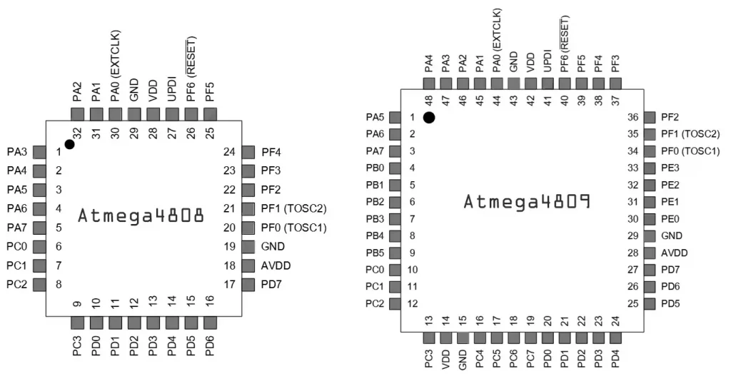
Both microcontrollers belong to the megaAVR®0 series, which differs fundamentally from the “traditional” AVR® series. For example, programming is done via UPDI (Unified Program Debug Interface) and not as usual via ISP or using the Optiboot bootloader via the UART interface. This is why the boards discussed here do not have a USB-to-serial adapter, but a UPDI programmer. UPDI is a 1-wire interface that you may recognize from my article about the megaTinyCore package from Spence Konde.
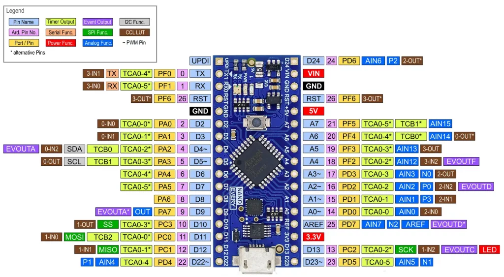
Pinout Arduino Nano Every

As you can see, the pins of the ATmega4809 are only partially available on the Arduino Nano Every Board. The rest is lost. In some cases, however, you can use PORTMUX to reassign the functions of non-available pins to existing pins.
The pin designations and pin numbers (light blue / pink) essentially correspond to those of the ATmega328P-based Arduino Nano. However, there are some differences:
- A6 and A7 can be used as I/O pins.
- A4 and A9 have two pin numbers, namely 18/22 and 19/23.
- AREF’s pin number is 39, but only when using the MegaCoreX package (therefore not mentioned in the pinout).
The port pins Pxy on which the Arduino pins are based are entirely different from those of the Arduino Nano or Arduino UNO. Sketches that address the ports directly must be rewritten if you transfer them to the Arduino Nano Every.
We will come to the other functions, such as TCA0-x or EVENTy, in the course of this article.
Pinout “Nano 4808”
The pinout diagram of the “Nano 4808” differs from the Arduino Nano Every as follows:
- Pins 22 and 23 are separate, pin 24 is added.
- The PWM pins are assigned differently.
- A UPDI pin is available. You can therefore use a UPDI-capable programmer such as the Atmel ICE instead of the existing on-board programmer, provided the board package has implemented the programmer.
- The port pins on which the Arduino pins are based are different again.
Board packages
I will not explain here in detail how to install board packages. Instructions can be found here, for example.
Board packages for the Arduino Nano Every
The easiest way is to install the “Arduino megaAVR Boards” package, as you do not need to enter an additional board manager URL in the settings. After installation, select the Arduino Nano Every as the board and set the option “None (ATMEGA4809)” under Tools → “Registers emulation”.
As an alternative, I recommend the MegaCoreX package, as it contains libraries for many of the ATmega4809 functions that the standard package does not have. This is particularly useful for those who do not want to deal with registers. You can apply many more settings with this package, such as conveniently converting the reset pin into a normal I/O pin or changing the clock rate. The documentation on GitHub is exemplary. You can find installation instructions here. Don’t worry, it’s done in just a few minutes.
After installation, make the following settings in the Tools menu:
- Board: MegaCoreX → ATmega4809
- Pinout: Nano 4809
- Programmer: JTAG2UPDI
The rest is best left unchanged for now.
Board packages for the “Nano 4808” (Thinary)
I tried two options for the “Nano 4808”. One of them was again the MegaCoreX package, but I also tried the ThinaryArduino package. Do yourself a favor and take the MegaCoreX package!
I do not recommend the ThinaryArduino package, as it is apparently not really maintained. It works in principle, but has some special features:
- Serial must be replaced by Serial1.
analogWrite()is only available on pins A6 and A7.- The documentation leaves a lot to be desired.
Using Reset and AREF pins as GPIO
You can use the AREF pin as a GPIO without any further action. The only limitation: It has a higher capacitance than other pins and is therefore somewhat less responsive. The MegaCoreX package has assigned its own number for the pin, namely 39 for the Arduino Nano Every and 25 for the “Nano 4808”. When using the megaAVR package, you could use it directly via port manipulation (PD7).
Since the ATmega4808/4809 is flashed via UPDI, you do not need the reset pin to upload the sketches. The MegaCoreX allows you to set the pin as a GPIO via the Tools → Reset menu. But be careful: If you configure the pin as OUTPUT and press the reset button, you will create a short circuit!
With the megaAVR package, you can apply this change in the boards.txt file. On my computer it is under: “C:\Users\Ewald\AppData\Local\Arduino15\packages\arduino\hardware\megaavr\1.8.8”. Replace the following line in the file:
nona4809.bootloader.SYSCFG0=0xC9 by:
nona4809.bootloader.SYSCFG0=0xC1.
This clears the RSTPINCFG bit (no. 3) in the SYSCFG0 register as part of the next upload. As the register can only be written to via UPDI, you have to take the detour via boards.txt. But only go for it if you know exactly what you’re doing!
Getting Started
If you limit yourself to the Arduino functions, your sketches should work as usual. It all “feels like Arduino Nano”.
This could be the end of this article. But there is still the exciting world of the megaAVR0 series to discover beneath the Arduino surface. Nevertheless, a little familiarization is required, even if you should already have experience with register programming of AVR microcontrollers. Here is a simple blink sketch as a taster (Arduino Nano Every):
void setup() {
    PORTE.DIRSET = PIN2_bm; // set PE2 (D13, LED_BUILTIN) to OUTPUT
}

void loop() {
    PORTE.OUTSET = PIN2_bm;  // set PE2 to HIGH
    delay(200);
    PORTE.OUTCLR = PIN2_bm;  // set PE2 to LOW
    delay(200);
}
For the “Nano 4808”, replace PORTE with PORTC to make the board LED flash.
A statement like PORTE |= (1<<PE2) generates an error message that “PE2” is not defined.
Register programming in C for the megaAVR® series
I will now try to explain the register programming briefly. For more details, please refer to the application note TB3262 from Microchip.
The register concept of the megaAVR series can also be found for the megaTiny® series. If you have worked through this article, you can also use your knowledge there.
Register
The registers are organized as structures (data type struct), which you can see from the dot notation in the blink sketch. The name of the structure is the module, the registers are elements of this structure, e.g.
- PORTE.DIRSET:
- Module: PORTE
- Register: DIRSET
Bit Masks and Bit Group Configuration Masks
To understand bit masks and bit group configuration masks, let’s take a look at the Control A Register (CTRLA) of Timer B1 as an example. The module is called TCB. However, as the ATmega4809 has four identical Timer B (0, 1, 2, 3), the number is appended to the module name, in general term: “MODULNAMEn.REGISTERNAME”. The CTRLA register of Timer B1 is therefore called: TCB1.CTRLA.
The TCBn.CTRLA registers contain various bits and the CLKSEL bit group:
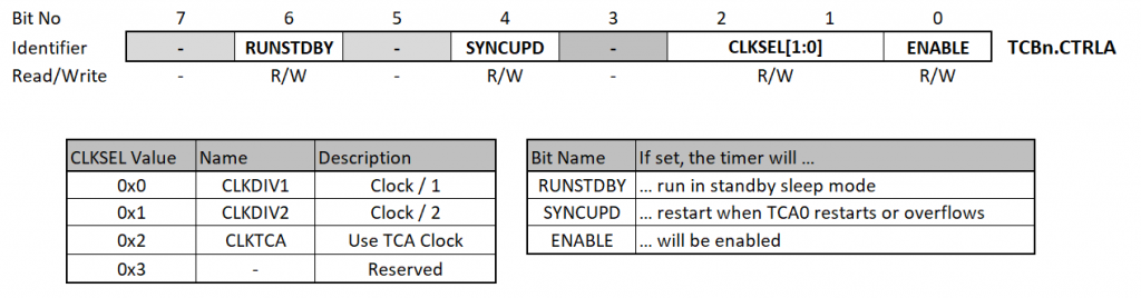
Bit masks are used to set single bits. Their names are formed according to the following scheme:
- MODUL_BIT_bm
The module number is omitted. To set the ENABLE bit for Timer B1:
TCB1.CTRLA |= TCB_ENABLE_bm;
The bit group configuration masks are used for bit groups (also known as bit fields), the names of which are formed as follows:
- MODUL_BITGRUPPE_CONFIGURATION_gc
As an example, we set the TCA clock as clock source for Timer B1:
TCB1.CTRLA |= TCB_CLKSEL_CLKTCA_gc;
CLKTCA corresponds to the CLKSEL value 0x2 or 0b10. In the register, CLKSEL is located at bit position 1 and 2, i.e. it is shifted 1 bit to the left. This is why the value of TCB_CLKSEL_CLKTCA_gc is 0x4 or 0b100.
If you want to mask the bit group TCB_CLKSEL, you can use the bit group mask. Here in the general form:
- MODUL_BITGRUPPE_gm
The value of TCB_CLKSEL_gm is 0x6 or 0b110, as you can easily check with Serial.println(TCB_CLKSEL_gm, BIN).
Bit Positions and Bit Group Positions
In addition, there are the bit and bit group positions:
- MODUL_BIT_bp
- MODUL_BITGRUPPE_gp
Unsurprisingly, they indicate the position of the bit or bit group in the register. So if you want to determine the current CLKSEL value of timer TCB1, you could do it like this:
Serial.println( ((TCB1.CTRLA & TCB_CLKSEL_gm) >> TCB_CLKSEL_gp) );
It may all sound a little complicated at first, but you soon get used to this type of notation. It involves a certain amount of writing, but it pays off because the code is still easy to understand even after a few months.
If you want to see how the structures for the modules and registers are set up, then take a look at “C:\Program Files (x86)\Arduino\hardware\tools\avr\avr\include\avr\iom4809.h” or “…iom4808.h”.
Orientation in the Data Sheet
This new way of programming registers takes some getting used to at first. The ATmega4808/4809 data sheet will help you find your way around. It is organized according to the modules and for each module there is a “Register Summary” with links to the individual registers.

I/O Control – PORTx Module
PORTx Register
DIR, OUT and IN registers
As demonstrated by the register summary above, there are a number of registers whose names begin with “DIR” or “OUT”. The “DIR …” registers control which pins are used as INPUT or OUTPUT. With the help of the “OUT …” registers you set the pin level, i.e. HIGH or LOW. The second part of the name means:
- SET: sets bits in OUT and DIR → OUTPUT or HIGH
- CLR: clears bits in OUT and DIR → INPUT or LOW
- TGL: toggles the status.
You can also write directly to the DIR and OUT registers, but the beauty of OUTSET, OUTCLR, OUTTGL and their “DIR” counterparts is that the instructions are pin-selective. Example:
PORTx.OUT = PINy_bm;sets pin y of port x to HIGH and all other pins of port x to LOW.PORTx.OUTSET = PINy_bm;only acts on pin y, i.e. the statement corresponds toPORTx.OUT |= PINy_bm;.
You can read the status of the pins from the IN registers (digitalRead(), so to speak). However, if you write a bit to the PORTx.IN register, the corresponding bit is toggled in PORTx.OUT. The IN register is the counterpart to the PINx register of traditional AVR microcontrollers.
Control Register PINxCTRL
Each pin has its own control register, namely PINxCTRL:

The INVEN bit allows you to invert the INPUT and OUTPUT values. PULLUPEN activates the internal pull-up resistor. With ISC you can define the interrupt conditions or switch off the digital function of the pin completely (INPUT_DISABLE):
![ISC[2:0] Bit Group Configurations](https://wolles-elektronikkiste.de/wp-content/uploads/2023/11/PINxCTRL_ISC_table.webp)
Example Sketches for PORTx
Switching Pins
I’ll come back to the blink sketch and show that there are other ways to achieve the same effect:
void setup() {
    PORTE.DIRSET = PIN2_bm; // set PE2 (D13) to OUTPUT
    // PORTE.DIR |= (1<<2);
    // PORTE.DIR |= (1<<PIN2_bp); // bp = bit position
}

void loop() {
    PORTE.OUTSET = PIN2_bm;  // set PE2 to HIGH
    // PORTE.OUT |= PIN2_bm;
    delay(200);
    PORTE.OUTCLR = PIN2_bm;
    // PORTE.OUT &= ~PIN2_bm;
    delay(200);

    // Alternative: toggle pin:
    // PORTE.OUTTGL = PIN2_bm;
    // delay(200);
}
I think the alternatives are fairly self-explanatory. And as already mentioned, to adapt the code to a “Nano 4808”, swap PORTE for PORTC.
Reading Pin Levels
Here is an example of how you can read the level of individual pins:
void setup() {
    Serial.begin(115200);
    PORTB.DIRCLR = PIN2_bm; // PB2 = D5 (for the Nano4808 select a different pin)
}

void loop(){
    if(PORTB.IN & PIN2_bm){
        Serial.println("HIGH");
    }
    else{
        Serial.println("LOW");
    }
    delay(1000);
}
Setting up Interrupts
The following is a simple example of an external interrupt at PB2 (=D5 on the Nano Every). Note that the interrupt is not automatically cleared by calling the ISR. You must “manually” clear the bit in the relevant interrupt flag register.
volatile bool event = false;

ISR(PORTB_PORT_vect){
    PORTB.INTFLAGS = PIN2_bm; // clear interrupt
    event = true;
}

void setup() {
    Serial.begin(115200);
    PORTB.DIRCLR = PIN2_bm;  // redundant in this case
    PORTB.PIN2CTRL = PORT_PULLUPEN_bm | PORT_ISC_BOTHEDGES_gc;
}

void loop(){
    if(event){
        Serial.println("Interrupt!");
        event = false;
    }
}
Virtual Ports
If you use port manipulation like PORTB.OUT = (1 << 2);, you should use the virtual port registers instead of the port registers. To do this, simply place a “V” before PORTx, i.e.: VPORTB.OUT = (1 << 2);. The virtual ports are copies of the ports in the lower address space. Port manipulations are performed faster with virtual ports. It took 629 milliseconds to execute the following code:
for(unsigned long i=0; i<1000000;i++){
        PORTE.OUT = 0;
        PORTE.OUT = (1<<2);
}
The same code, only with VPORTE instead of PORTE took 503 milliseconds. These are not major differences, but they are differences nonetheless.
The VPORT registers available are DIR, OUT, IN and INTFLAGS.
Reassigning Inputs / Outputs – PORTMUX Module
The registers of the PORTMUX module allow you to assign a series of inputs and outputs to alternative pins. Here is the register summary:
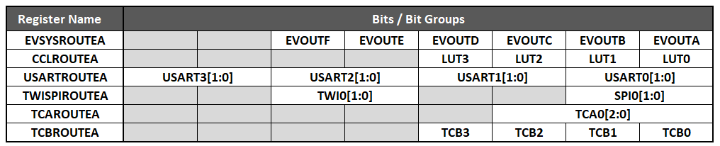
As an example, we redirect the Timer A outputs. The relevant PORTMUX register is TCAROUTEA. The bit group configuration mask for TCA0[2:0] is PORTn with n = A to F. You would therefore assign the Timer A output pins to Port B in this way:
PORTMUX.TCAROUTEA = PORTMUX_TCA0_PORTB_gc;
And this is exactly what is implemented on the Arduino Nano Every, both with the megaAVR and the MegaCoreX package. On the “Nano 4808”, the Timer A outputs are redirected to Port D.
If you want to redirect other inputs or outputs, you only need to search for the corresponding bit masks or bit group configuration masks.
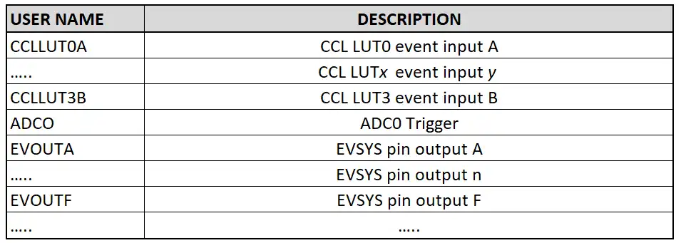
The Event System – EVSYS Module
The event system is really cool! It allows the peripherals, i.e. timers, ADC, USART, etc., to send signals to other peripherals without involving the CPU. Later, I will show you an example of how a timer can regularly trigger ADC measurements. Normally, you would realize this via delay(), millis() or interrupts. All these options take a certain amount of time and can make the code complex.
8 channels (Channel0 to Channel7) are available for transmitting the signals. The sender of the signal is called the generator, the receiver is the user. Most users have their own event control register in which further settings can be made. These registers are part of the peripheral modules.
EVSYS Register
CHANNELn Register – Definition of the Generator
In the CHANNELn registers (with n = 0 to 7) you define the generator:

Most generators can utilise all channels. But there are also exceptions. For example, the pins of Port A can only use channels 0 and 1. Here is a small extract from the table in the data sheet (section 14.5.2):

Register USERn – Definition of Users
You define the event users in the USERn tab:

Replace the “n” in USERn with the name of the user. The complete table can be found in the data sheet in section 14.3.2.4. Here is a snippet:
A simple Event System Example
For a better understanding, let’s take a look at a small example. For the Arduino Nano Every, connect a button to PB0 (D9) that pulls the pin to LOW when pressed. Connect a suitable LED to PB2 (D5).
Now we use the PB0 as event generator and EVOUTB (PB2 / D5) as event user. Channels 0 and 1 are available for Port B. In the example, we use Channel 0.
void setup() {
    PORTB.DIRSET = PIN2_bm; // PB2 (D5) as OUTPUT
    PORTB.DIRCLR = PIN0_bm; // PB0 (D9) as INPUT
    PORTB.PIN0CTRL = PORT_PULLUPEN_bm;

    EVSYS.CHANNEL0 = EVSYS_GENERATOR_PORT1_PIN0_gc;  // PB0 is event generator for channel 0
    EVSYS.USEREVOUTB = EVSYS_CHANNEL_CHANNEL0_gc;  // EVOUTB is user of event channel 0
}

void loop(){}
PB5, or EVOUTB, reflects the status of PB0. The LED lights up in the normal state and switches off when the button is pressed. This may not be impressive at first glance, but at second glance it is. We do not query the level of PB0, nor have we set up an external interrupt for this purpose. In addition, there are no instructions for switching the LED in the running program. The processes are all controlled in the background without your running program having to do anything. More useful applications will follow later.
Variant for the “Nano 4808”
Rewriting the sketch for the “Nano 4808” is not difficult. This would be an option:
void setup() {
    PORTA.DIRSET = PIN2_bm; // PA2 (D4)
    PORTA.DIRCLR = PIN0_bm;  // PA0 (D2)
    PORTA.PIN0CTRL = PORT_PULLUPEN_bm;

    EVSYS.CHANNEL0 = EVSYS_GENERATOR_PORT0_PIN0_gc;
    EVSYS.USEREVOUTA = EVSYS_CHANNEL_CHANNEL0_gc;
}

void loop(){}
The Timers of the Arduino Nano Every / “Nano 4808”
The ATmega4809 has:
- One 16-bit Timer A (TCA0)
- four 16-bit Timers B (TCB0, TCB1, TCB2, TCB3),
- a Real-Time Counter (RTC),
- a Periodic Interrupt Timer (PIT),
- and a Watchdog Timer (WDT).
The ATmega4808 differs only in that it has three Timer B.
Timer A – Module TCAn
First, a few general comments on Timer A:
- The system clock is the clock source for Timer A, but it can be slowed down with a divider you set in register TCA0.SINGLE.CTRLA.
- The megaAVR board package sets the divider of Timer A to 64 and uses the Timer A clock for Timer B. Timer B3 is in turn responsible for time-dependent functions such as
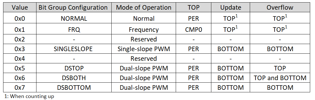
millis()ordelay(). You should therefore not change the divider if you are using the Arduino megaAVR package. The Timer A clock is thus set to 16000000 MHz / 64 = 250 kHz. The MegaCoreX package also uses Timer B3 (or B2 for the “Nano 4808”) fordelay()andmillis(). However, Timer B3 uses the system clock, so you can adjust the Timer A divider without side effects on Timer B. - In Normal (single) Mode, Timer A counts up to the maximum value PER. Three compare channels are available. The compare values are called CMP0, CMP1 and CMP2.
- In split mode, the 16-bit timer turns into two 8-bit timers with 3 compare values each.
- You address the registers for the Normal Mode with TCA0.SINGLE.Registername, and the registers for Split Mode with TCA0.SPLIT.Registername.
- By default, the outputs for Timer A are assigned to Port B on the Arduino Nano Every. Assignment to other ports is possible, but this redirection always applies to all output pins. Pin 0 is responsible for Channel 0 (TCA0-0), pin 1 for Channel 1 (TCA0-1) and pin 2 for Channel 2 (TCA0-2). In Split Mode, this scheme continues accordingly with Pin 3 for Channel 3 (TCA0-3), etc. On the “Nano 4808”, the Timer A outputs are assigned to Port D.
Timer A Registers for Normal (Single) Mode
Some registers are identical in Normal and Split Mode. I have noted this accordingly.
This article is not a complete register documentation. I recommend that you also take a look at the data sheet when reading this article.
Control A Register TCAn.CTRLA
In the control register CTRLA you set the clock divider and enable Timer Counter A.

The CLKSEL (Clock Select) bit group defines the divider. The following bit group configuration masks are available for selection:
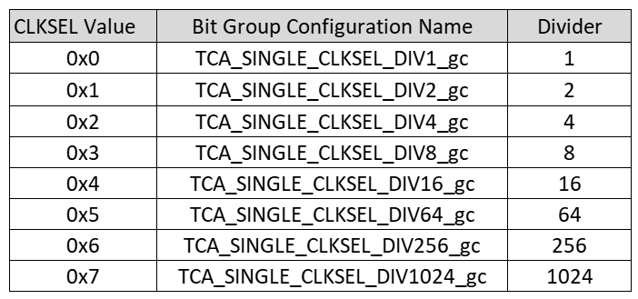
Use the ENABLE bit to enable TCA0. You can check the setting of CTRLA with Serial.println(TCA0.SINGLE.CTRLA). The output should be 0b1011, i.e. the timer is enabled, and the divider is 64, so you do not need to enable the timer yourself. And once again: When using the megaAVR package, you should not change this setting.
Control B Register TCAn.CTRLB

Setting the Compare n Enable Bits (CMPnEN) enables the Compare Channel outputs. I will not go into the Auto Lock Update Bit (ALUPD) here. The bit group WGMODE[2:0] defines the Wave Form Generation Mode:
Take it as it is for now, it will become clearer later.
Control D Register TCAn.CTRLD
The Split Mode is set in the Control D register. It is not relevant whether you make the setting via TCA0.SINGLE.CTRLD or TCA0.SPLIT.CTRLD.

Interrupt Control Register TCAn.INTCTRL
In the Interrupt Control Register, you set which interrupts are to be activated. Interrupts are available for compare matches and overflow:

The Interrupt Flag Register INTFLAGS is similar to INTCTRL and uses the same bit names and positions.
Event Control Register TCAn.EVCTRL
You can set Timer A so that it is not controlled by the system clock but by external events. To do this, set the “Enable Count On Event Input” bit CNTEI in the Event Control Register EVCTRL.

Use the Bit Group Configuration EVACT to select which events are counted and how they are counted:
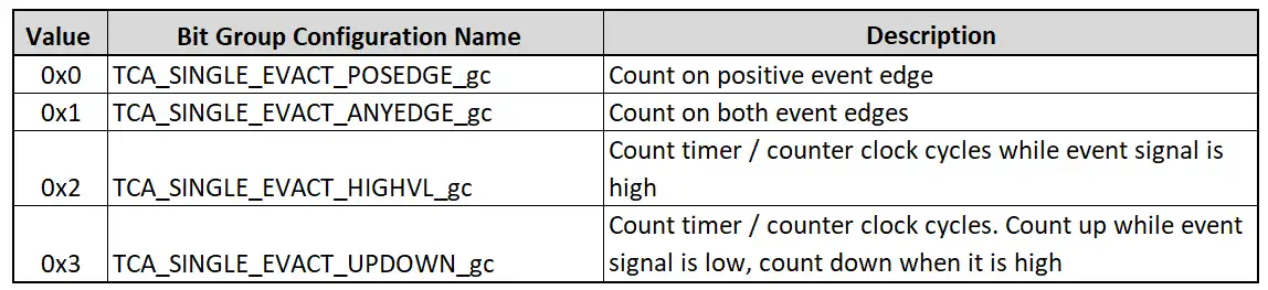
With the first two settings, you count the edges, i.e. the number of events. With the other two settings, the system clock (with divider if necessary) is used to count for as long as the state caused by the event lasts.
Further registers
Then there are a number of other registers that only contain numbers:
- CNT (16 bit): is the counter register for timer A.
- PER (16 bit): is the TOP value for most wave form generation modes.
- CMP0, CMP1, CMP2 (16 bit): contain the compare values.
- PERBUF: you can write PER directly to the PER register. This can lead to undefined states if PER is changed in the middle of a PWM period, for example. When transferring from PERBUF to PER, the system waits until the current PER value is reached. So this route is safer.
- CMP0BUF, CMP1BUF, CMP2BUF: see PERBUF.
In normal (single) mode, Timer A counter has a size of 16 bits. However, it can also be split into two 8-bit timers (Split Mode). In Normal Mode there are three Compare Channels available, in Split Mode there are six. Accordingly, Timer A can be used to provide 3 or 6 PWM outputs.
The board packages for the Arduino Nano Every discussed here assign the Timer A outputs to PORTB and use them for analogWrite(). As only PB0 (pin 9), PB1 (pin 10) and PB2 (pin 5) are available as board pins, there are only these three analogWrite() pins that are controlled by Timer A.
The MegaCoreX board package assigns the Timer A to Port D when using the “Nano 4808”. As PD0 to PD5 are all brought out as board pins and Split Mode is activated, six PWM pins are available (through Timer A).
Example sketches for Timer A in Normal Mode
After all the theory, let’s have some example sketches.
Overflow Interrupt
We start quite simply with an overflow interrupt. We use this to toggle the board LED of the Arduino Nano Every.
ISR(TCA0_OVF_vect){  // ISR für den Timer A over
    TCA0.SINGLE.INTFLAGS = TCA_SINGLE_OVF_bm; // Clear the interrupt flag (needed!)
    PORTE.OUTTGL = PIN2_bm; // Toggle PE2 (Board-LED)
}

void setup() {
    PORTE.DIRSET = PIN2_bm; // PE2 auf OUTPUT
    // TCA0.SINGLE.CTRLA = TCA_SINGLE_CLKSEL_DIV64_gc | TCA_SINGLE_ENABLE_bm; // redundant
    // TCA0.SINGLE.CTRLB = 0; // no output, wave form: normal; redundant
    TCA0.SINGLE.PERBUF = 49999; // Set TOP for Timer A
    TCA0.SINGLE.INTCTRL = TCA_SINGLE_OVF_bm; // enable Timer A overflow interrupt
}

void loop() {}
With a clock rate of 16 MHz, a divider of 64 and a PER of 49999 (= 50000 steps), the overflow frequency is 16000000 / 64 / 50000 = 5 Hz.
If you want to use the sketch on the “Nano 4808”, simply replace PORTE with PORTC.
Single Slope PWM
In the next example, we use the Arduino Nano Every to generate a PWM signal with a frequency of 250 Hz and a duty cycle of 20 % at PB1 / D10. We achieve a frequency of 250 Hz by setting PER to 999 (at 16 MHz). PB1 is the output of compare Channel 1, so we have to set the CMP1EN bit accordingly. The duty cycle is CMPn / (PER +1).
void setup() {
    PORTB.DIRSET = PIN1_bm;  // PB1 (D10)
    TCA0.SINGLE.CTRLD &= ~TCA_SINGLE_SPLITM_bm; // needed for the MegaCoreX board package
    TCA0.SINGLE.PERBUF = 999;
    TCA0.SINGLE.CMP1BUF = 200;
    TCA0.SINGLE.CTRLB = TCA_SINGLE_CMP1EN_bm | TCA_SINGLE_WGMODE_SINGLESLOPE_gc;
}

void loop() {}
To translate the sketch for use on the “Nano 4808” board, replace Port B with D. You will obtain the PWM signal on pin A1. If you are not sure why this is the case, take another look at the pinout diagrams.
Please note that the MegaCoreX package has Split Mode activated by default. You must therefore deactivate it. I’ll come back to that shortly.
Counting Events
In this example for the Arduino Nano Every, we control Timer A via events. A rising edge at PB1 (pin 10) serves as an event. To do this, connect PB1 to GND via a push-button. PB1 is pulled to HIGH by its internal pull-up resistor. The event is therefore generated when the button is released. You can also invert the logic, but then you will need an additional external pull-down resistor.
The following sketch informs us when the button has been pressed 10 or 20 times:
volatile bool tca0Ovf = false;  // Flag für TCA OVF
volatile bool cmp0Match = false;  // Flag für CMP0 Match

ISR(TCA0_OVF_vect){
    TCA0.SINGLE.INTFLAGS = TCA_SINGLE_OVF_bm; /* Clear the interrupt flag */
    tca0Ovf = true;
}

ISR(TCA0_CMP0_vect){
    TCA0.SINGLE.INTFLAGS = TCA_SINGLE_CMP0_bm; /* Clear the interrupt flag */
    cmp0Match = true;
}

void setup() {
    Serial.begin(115200);
    PORTB.DIRCLR = PIN1_bm; // PB1 (Pin 10) as input
    PORTB.PIN1CTRL = PORT_PULLUPEN_bm; // Pullup enable
    EVSYS.CHANNEL1 = EVSYS_GENERATOR_PORT1_PIN1_gc; // PB1 as event generator
    EVSYS.USERTCA0 = EVSYS_CHANNEL_CHANNEL1_gc;  // TCA0 as event user
    TCA0.SINGLE.CTRLD &= ~TCA_SINGLE_SPLITM_bm;  // Set single mode
    TCA0.SINGLE.CTRLA = 0;  // switch off the timer, set clock divider to DIV1
    TCA0.SINGLE.PER = 19;  // TCA0 counter limit
    TCA0.SINGLE.CMP0 = 9;  // Compare match value
    TCA0.SINGLE.CNT = 0;  // Set TCA0 counter to 0
    TCA0.SINGLE.EVCTRL = TCA_SINGLE_EVACT_POSEDGE_gc | TCA_SINGLE_CNTEI_bm; // count pos. edge of events (RISING) & enable event count
    TCA0.SINGLE.CTRLB = TCA_SINGLE_WGMODE_NORMAL_gc; // normal mode => TOP = PER
    TCA0.SINGLE.INTFLAGS = TCA_SINGLE_OVF_bm; // clear the overflow interrupt flag
    TCA0.SINGLE.INTCTRL = TCA_SINGLE_CMP0_bm | TCA_SINGLE_OVF_bm; // enable CMP0 and OVF interrupts
    TCA0.SINGLE.CTRLA = TCA_SINGLE_ENABLE_bm;
}

void loop(){
    if(cmp0Match){
        Serial.println("Key has been pressed 10 times");
        cmp0Match = false;
    }

    if(tca0Ovf){
        Serial.println("Key has been pressed another 10 times");
        Serial.println("Timer/Counter A restarts");
        tca0Ovf = false;
    }
    // Serial.println(TCA0.SINGLE.CNT);
    // delay(100); // delay won't work with the Arduino board package!
}
I have tried to explain the code in the comments. I hope that is sufficiently understandable. However, a few annotations are still necessary:
- Split Mode is preset in the MegaCoreX package. We therefore delete the SPLITM bit in CTRLD.
- We switch off Timer A so that it does not disturb us during the settings.
- We are informed via Compare 0 Interrupt and Overflow Interrupt when the button has been pressed ten or twenty times.
- The interrupts are only triggered when CMP0 and PER are exceeded. This is why CMP0 is 9 and PER is 19.
- Setting the Compare 0 register and the PER register via the buffer registers (CMP0BUF, PERBUF) does not work here, as the new PER value is only updated once the old PER value has been reached. In the worst case, you would have to press the button 216 times until this is the case.
- If you use the megaAVR package,
delay()will no longer work for the reasons already mentioned several times. MegaCoreX does not have this problem.
To adapt the sketch for the “Nano 4808”, you could replace PB1 by PA1 (pin 3) and then change the event generator to EVSYS_GENERATOR_PORT0_PIN1_gc.
Timer A register in Split Mode
In Split Mode, Timer A is divided into a high and a low section. Accordingly, there is an 8-bit HCNT and an 8-bit LCNT register instead of the 16-bit CNT register. These two counter registers count independently of each other. The PER register and the compare registers are also split. PER turns into HPER and LPER, CMPn turns into HCMPn and LCMP and so on.
The outputs for Timer A in Split Mode are activated in the Control B register (TCA0.SPLIT.CTRLB):

The LCMPnEN bits are responsible for the TCA0-n outputs, the HCMPnEN bits for the TCA0-(n+2) outputs.
You can set interrupts for the low Compare Channels in the Control D register. No interrupts are available for the high Compare Channels.
In Split Mode, the HCNT and LCNT registers count downwards. Accordingly, there are no overflow interrupts, but underflow interrupts (“UNF”). The bits for activating the interrupts are HUNF and LUNF.

The corresponding names of the interrupt vectors are formed according to the scheme TCA0_Interruptbit_vector, e.g. TCA0_LCMP1_vector.
Example sketches for Timer A in Split Mode
Split Mode Timer A – Arduino Nano Every
Then we try Timer A in Split Mode and start with the Arduino Nano Every. The aim is to generate a PWM signal with a duty cycle of 25 % at PB0 (TCA0-0). The low counter of Compare Channel 0 is responsible for this.
void setup() {
    PORTB.DIRSET = PIN0_bm;  // PB0 (D9 = Output)
    TCA0.SPLIT.CTRLD = TCA_SPLIT_SPLITM_bm; // needed for the Arduino board package
    TCA0.SPLIT.LPER = 255;
    TCA0.SPLIT.LCMP0 = 64; // Duty cycle = 64 / (255 + 1) * 100 = 25 %
    TCA0.SPLIT.CTRLB = TCA_SPLIT_LCMP0EN_bm;
}

void loop() {}
As PB3, PB4 and PB5 are not available as board pins, you can only use LCNT for PWM, unless you assign the TCA0 outputs to another port with PORTMUX.TCAROUTEA = PORTMUX_TCA0_PORTn_gc;.
Split Mode Timer A – “Nano 4808”
The MegaCoreX package for the “Nano 4808” assigns the TCA0 outputs to Port D. Here we can directly use all six PWM channels of Timer A in Split Mode. Here is an example of a PWM signal at PD4 (TCA0-4 = D22):
void setup() {
    PORTD.DIRSET = PIN4_bm;  // PD4 (D22 = Output)
    // TCA0.SPLIT.CTRLD = TCA_SPLIT_SPLITM_bm;
    TCA0.SPLIT.HPER = 255;
    TCA0.SPLIT.HCMP1 = 64;
    TCA0.SPLIT.CTRLB = TCA_SPLIT_HCMP1EN_bm;
}

void loop() {}
analogWrite() on the 4808 / 4809 boards
The Arduino Nano Every and the “Nano 4808” or their board packages basically do what we have just done to provide analogRead() pins. The Arduino Nano Every uses TCA0-0, TCA0-1 and TCA0-2 and the Nano 4808 TCA0-0 to TCA0-5. The other analogRead() pins are Timer B outputs.
If you want to mix your “self-made” PWM outputs on some pins with analogRead() on other pins in one sketch, then you have to make sure that this is all compatible. If you set PER, HPER or LPER, this can have a direct impact on analogRead(), depending on the board or board package. The same applies if you switch to Normal or Split Mode, or if you assign the TCA outputs to another port.
Timer B – TCBn Module
The Arduino Nano Every, or the ATmega4809 on which it is based, has four 16-bit Timers B (TCB0 to TCB3). The “Nano 4808” has three of these timers (TCB0 to TCB2). The differences to Timer A become clear when discussing the registers.
For time measurements (millis(), delay()) the board packages use the TCB3 (Arduino Nano Every) or the TCB2 (“Nano 4808”). Changes to the settings of these timers lead to problems with the functions mentioned.
TCB0 and TCB1 are used by all boards and board packages discussed here to provide analogWrite() pins. If you use these timers for other purposes or change the settings, you will lose the analogWrite() function of the affected pins.
No outputs are available for TCB2 and TBC3 on the Arduino Nano Every, as the relevant pins PC0/PB4 and PC1/PB5 are not implemented.
Timer B Register
Once again, I would like to point out that this article does not cover all existing registers.
Control A Register TCBn.CTRLA
The most important settings in the Control A registers of Timer B are the clock rate (CLKSEL[2:0]) and enable. The system clock, the system clock divided by two or the clock of timer A can be selected as the clock rate.
Control B Register TCBn.CTRLB
In the Control B Register, you define one of the eight Count Modes (data sheet calls them “Timer modes”) that make the Timer B a versatile tool. For now, I will only list the count modes here, as they are best explained by the example sketches.

![CTNMODE[2:0] Bit Group Configurations](https://wolles-elektronikkiste.de/wp-content/uploads/2023/11/TCB_CTRLB_CNTMODE_TABLE.png)
The other bits have the following effects:
- ASYNC (Asynchronous Enable): allows asynchronous updates of the TCB output signal in Single Shot Mode.
- CCMPINIT (Compare / Capture Pin Initial Value): sets the initial level of the output pin (0 = LOW, 1 = HIGH).
- CCMPEN (Compare / Capture Output Enable): activates the Compare / Capture Output. In contrast to Timer A, there is only one Compare Output per Timer B, but you have a larger number of timers.
Interrupt Control Register TCBn.INTCTRL
The Interrupt Control Register is simple. You can activate the Capture Interrupt there, that’s all. The condition for triggering the interrupt depends on the Count Mode. I will come back to this in the examples. An overview can be found in the data sheet in section 21.5.5.

The interrupt vector is called TCBn_INT_vect and not – as one would expect – TCBn_CAPT_vect. Unfortunately, this is somewhat confusing.
Event Control Register TCBn.EVCTRL
The effect of the EDGE bit in the Event Control Register EVCTRL also depends on the Count Mode. Wait for the examples or take a look at the overview in the data sheet in section 21.5.3.
The FILTER bit activates a noise filter that ensures that the event status must be constant for four clock cycles before the event is considered valid.
The Capture Event Input Enable Bit CAPTEI activates the input capture event. In contrast to Timer A, Timer B cannot count edges (events), but the edge starts or stops the counter.

Further registers
The 16-bit register CNT contains – unsurprisingly – the Counter status of Timer B. Strictly speaking, there are two registers that you can address together via TCBn.CNT or separately via TCBn.CNTL and TCBn.CNTH.
As the name suggests, the Capture / Compare Register CCMP has various tasks. As a Compare Register, it controls interrupts and PWM, as a Capture Register it records counter readings as measured values.
Example sketches for Timer B
We will now go through example sketches for each Count Mode. The sketches are written for the Arduino Nano Every. The translation to the “Nano 4808” should not be difficult.
periodic interrupt
In Periodic Interrupt mode, the timer counts down to CCMP, triggers the CAPT interrupt (if activated) and starts again from the beginning. In the following example sketch, we use the CAPT interrupt to toggle the board LED. As we use the Timer A clock (default setting DIV64) and set CCMP to 50000, the toggle frequency is: 16000000 / (64 * 50000) = 5 Hertz.
ISR(TCB0_INT_vect){
    TCB0.INTFLAGS = TCB_CAPT_bm; /* Clear the interrupt flag */
    PORTE.OUTTGL = PIN2_bm; /* Toggle PE2 (D13 / LED-BUILTIN) */
}

void setup() {
    PORTE.DIRSET = PIN2_bm;
    PORTE.OUTSET = PIN2_bm;
    // TCA0.SINGLE.CTRLA |= TCA_SINGLE_CLKSEL_DIV1024_gc;
    TCB0.CCMP = 50000; // Toggle frequency = 5 Hz
    TCB0.INTCTRL = TCB_CAPT_bm;
    TCB0.CTRLA = TCB_CLKSEL_CLKTCA_gc | TCB_ENABLE_bm; // use TCA clock / enable
    TCB0.CTRLB = TCB_CCMPEN_bm;
}

void loop() {}
If you uncomment line 9, you change the clock divider from 64 to 1024, i.e. by a factor of 16. This reduces the toggle frequency to 0.3125 Hz (→ period 3.2 s). But don’t forget: changing the timer A clock leads to problems with delay() & Co. when using the Arduino megaAVR board package for the Arduino Nano Every. This is not a problem for the MegaCoreX package.
8-Bit PWM mode
PWM signals are easy to create using Timer B. The lower byte of the CCMP comparison register, namely CCMPL, determines the PWM frequency in conjunction with the Timer B clock. The duty cycle results from the ratio of CCMPH, the upper byte, to CCMPL. You can write to the CCMPH and CCMPL registers separately or together.
![\[ DutyCycle = \frac{\text{CCMPH}}{\text{CCMPL + 1}} \cdot 100\;\; [\%] \]](https://wolles-elektronikkiste.de/wp-content/ql-cache/quicklatex.com-be99fa4c24c04c98e3387cad8f98eb12_l3.png "Rendered by QuickLaTeX.com")
void setup() {
    PORTF.DIRSET = PIN5_bm; // PF5 = D3
    TCB1.CCMP = 0x40FF;
    /* Alternative:
    TCB1.CCMPL = 0xFF; // 255
    TCB1.CCMPH = 0x40; */ // 64
    TCB1.CTRLB |= TCB_CCMPEN_bm | TCB_CNTMODE_PWM8_gc;
    TCB1.CTRLA = TCB_CLKSEL_CLKTCA_gc | TCB_ENABLE_bm;
}

void loop(){}
In this example, we use the Timer A clock. This means that the frequency is 16 MHz / (64 * 256) = ~976.56 Hz. The duty cycle is 25%.
Single Shot Mode
In Single Shot Mode, the timer counts down to CCMP and then stops until it is reset to a value less than CCMP. To try out the following sketch, connect an LED to the TCB0 output PF4 (= pin 6).
void setup() {
    PORTF.DIRSET = PIN4_bm; // PF4 (D6) as output
    TCB0.CTRLA = 0; // disable TCB0
    TCB0.CCMP = 50000; // 0.2s signal length
    TCB0.CTRLB = TCB_CCMPEN_bm | TCB_CNTMODE_SINGLE_gc; // enable output / single shot mode
    TCB0.CTRLA = TCB_CLKSEL_CLKTCA_gc | TCB_ENABLE_bm; // enable TCB0, use TCA clock
}

void loop(){
    delay(1000);
    TCB0.CNT = 0; // restarts the counter
}
If your Arduino Nano Every is running at 16 MHz and you have not changed the Timer A clock, the LED will light up every second for 0.2 seconds.
Now we connect this with the Event System. To do this, connect a push-button to PB1 (pin 10), which you in turn connect to GND. Pushing the button (event generator) will start the TCB0 (event user).
ISR(TCB0_INT_vect){
    TCB0.INTFLAGS = TCB_CAPT_bm; /* Clear the interrupt flag */
}

void setup() {
    PORTF.DIRSET = PIN4_bm; // PF4 (D6) as output
    PORTB.DIRCLR = PIN1_bm; // PB1 (D10) as input
    PORTB.PIN1CTRL = PORT_PULLUPEN_bm;
    TCB0.CTRLA = 0; // disable TCB0
    EVSYS.CHANNEL1 = EVSYS_GENERATOR_PORT1_PIN1_gc; // PB1 as event generator
    EVSYS.USERTCB0 = EVSYS_CHANNEL_CHANNEL1_gc; // TCB0 as event user
    TCB0.CCMP = 50000; // 0.2s signal length
    TCB0.CTRLB = TCB_CCMPEN_bm | TCB_CNTMODE_SINGLE_gc; // single shot mode
    TCB0.EVCTRL = TCB_EDGE_bm | TCB_CAPTEI_bm; // counter starts at both edges / enable capture event input
    TCB0.INTCTRL = TCB_CAPT_bm; // enable interrupt
    TCB0.CNT = 50000; // prevents an unwanted, initial signal at PF4
    TCB0.CTRLA = TCB_CLKSEL_CLKTCA_gc | TCB_ENABLE_bm; // enable TCB0, use TCA clock
}

void loop(){}
According to the data sheet, chapter 21.5.3, the timer should only be triggered on a falling edge when the EDGE bit is set, i.e. when the button is pressed and not when it is released. However, the LED lights up for both events. Perhaps simply an error in the data sheet. If the EDGE bit is not set, the LED does what it should: it only lights up when it is released (rising edge). At least this applies as long as your button does not bounce.
You may have noticed line 16. If you comment out the line, you will see that the LED lights up with every reset. Starting the timer causes it to start counting at 0 and the LED lights up accordingly. If you set the timer counter to CCMP, this will not happen.
Input Capture Time-Out Check Mode
The Time-Out Check Mode only makes sense in combination with the Event System. In this mode, an event signal starts the timer at 0 and the next signal stops it. If EDGE is set, the falling edge starts the timer and the rising edge stops it. If EDGE is not set, the opposite applies. If the timer counter reaches CCMP, an interrupt is triggered and the timer counter continues to run.
We try this out as follows: a push-button connected to PB2 (D5) serves as an event generator that starts TCB0 in Time-Out Mode. As long as the button is pressed, TCB0 counts up. CCMP and the timer clock are set so that CCMP is reached after one second. If this occurs, an interrupt is triggered and the ISR toggles the board LED. If the button is released before CCMP is reached, there is no interrupt and the board LED does not toggle. The next time the button is pressed, the timer restarts at zero.
Under default conditions, CCMP is reached quickly. I have therefore slowed down Timer A and used it as clock source for Timer B. And once again, my warning: If you use the megaAVR board package for the Nano Every, this will affect all time functions. Nevertheless, you can of course just try out the sketch, as it does not contain delay() or millis(). This is not a problem for the MegaCoreX package anyway.
Here is the sketch reduced to the essentials:
#define TCB_TIMEOUT_VALUE (15625) // = 1s with the settings below

ISR(TCB0_INT_vect){
    TCB0.INTFLAGS = TCB_CAPT_bm; /* Clear the interrupt flag */
    PORTE.OUTTGL = PIN2_bm; /* Toggle PE2 (D13, LED_BUILTIN)*/
}

void setup() {
    Serial.begin(115200);
    PORTE.DIRSET = PIN2_bm; // PE2 (D13) as output
    PORTB.DIRCLR = PIN2_bm; // PB2 (D5) as input
    PORTB.PIN2CTRL = PORT_PULLUPEN_bm; // enable pull-up

    EVSYS.CHANNEL0 = EVSYS_GENERATOR_PORT1_PIN2_gc; // PE2 is event generator
    EVSYS.USERTCB0 = EVSYS_CHANNEL_CHANNEL0_gc; // TCB0 is event user

    TCB0.CCMP = TCB_TIMEOUT_VALUE;
    TCA0.SINGLE.CTRLA = TCA_SINGLE_CLKSEL_DIV1024_gc | TCA_SINGLE_ENABLE_bm; // slow down Timer A
    TCB0.CTRLB = TCB_CCMPEN_bm | TCB_CNTMODE_TIMEOUT_gc; // enable compare/capture output, time-out mode
    TCB0.INTCTRL = TCB_CAPT_bm; // enable capture interrupt
    TCB0.EVCTRL = TCB_EDGE_bm | TCB_CAPTEI_bm; // start counter on negative edge
    TCB0.CTRLA = TCB_CLKSEL_CLKTCA_gc | TCB_ENABLE_bm; // use timer A clock, enable TCB0
}

void loop(){}
With a 16 MHz system clock, a divider of 1024 and a CCMP of 15625, the counter reaches CCMP after 15625 * 1024 / 16000000 = 1 second. If you keep the button pressed, the counter continues to run and reaches CCMP every 65536 * 1024 / 16000000 = ~4.2 seconds.
So that you can see at which counter reading you have released the button, I have written a second version of the sketch:
#define TCB_TIMEOUT_VALUE (15625) // = 1s with the settings below
volatile bool keyReleased = false;

ISR(TCB0_INT_vect){
    TCB0.INTFLAGS = TCB_CAPT_bm; /* Clear the interrupt flag */
    PORTE.OUTTGL = PIN2_bm; /* Toggle PE2 (D13, LED_BUILTIN)*/
}

ISR(PORTB_PORT_vect){ // ISR for button release
    PORTB.INTFLAGS = PIN2_bm;
    keyReleased = true;
}

void setup() {
    Serial.begin(115200);
    PORTE.DIRSET = PIN2_bm; // PE2 (D13) as output
    PORTB.DIRCLR = PIN2_bm; // PB2 (D5) as input
    PORTB.PIN2CTRL = PORT_PULLUPEN_bm | PORT_ISC_RISING_gc; // pull-up / interrupt

    EVSYS.CHANNEL0 = EVSYS_GENERATOR_PORT1_PIN2_gc; // PE2 is event generator
    EVSYS.USERTCB0 = EVSYS_CHANNEL_CHANNEL0_gc; // TCB0 is event user

    TCB0.CCMP = TCB_TIMEOUT_VALUE;
    TCA0.SINGLE.CTRLA = TCA_SINGLE_CLKSEL_DIV1024_gc | TCA_SINGLE_ENABLE_bm; // slow down Timer A
    TCB0.CTRLB = TCB_CCMPEN_bm | TCB_CNTMODE_TIMEOUT_gc; // enable compare/capture output, time-out mode
    TCB0.INTCTRL = TCB_CAPT_bm; // enable capture interrupt
    TCB0.EVCTRL = TCB_EDGE_bm | TCB_CAPTEI_bm; // start counter on negative edge
    TCB0.CTRLA = TCB_CLKSEL_CLKTCA_gc | TCB_ENABLE_bm; // use timer A clock, enable TCB0
}

void loop(){
    if(keyReleased){
        Serial.println(TCB0.CNT);
        keyReleased = false;
    }
}
Input Capture On Event Mode
Now, we come to the four input capture modes that you can use to measure pulse widths and / or frequencies. For all examples, we use a PWM signal with a duty cycle of 75% on pin 10 (PB1) as the object to be measured, which we generate with analogWrite(10, 192). Pin 10 is the event generator, Timer B is the event user.
First, let’s look at the Input Capture On Event Mode. In this mode, the counter permanently counts from 0 to 65535, runs over and starts again from the beginning. Depending on whether you have set the EDGE bit or not, the timer writes the current counter value to the CCMP register on a falling or rising edge and triggers an interrupt. We read the CCMP register in the ISR of the Capture Interrupt. The difference to the last value is the period of the PWM signal, measured in timer counter increments.
In the event of a counter overflow between two interrupts, the difference is negative, and we have to add 65636.
volatile long cnt = 0;
volatile long lastCnt = 0;

ISR(TCB0_INT_vect){
    cnt = TCB0.CCMP - lastCnt; // Read the period
    lastCnt = TCB0.CCMP;
    if(cnt < 0){   // period is neg. when TCB0 was overflowed
        cnt += 65536;
    }
    TCB0.INTFLAGS = TCB_CAPT_bm; /* Clear the interrupt flag */

}

void setup() {
    Serial.begin(115200);
    analogWrite(10, 192); // the event source
    EVSYS.CHANNEL1 = EVSYS_GENERATOR_PORT1_PIN1_gc; // PB1 (Pin 10) is event generator
    EVSYS.USERTCB0 = EVSYS_CHANNEL_CHANNEL1_gc; // TCB0 is event user
    TCB0.CTRLA = 0; // Stop TCB0
    TCB0.CTRLB = TCB_CNTMODE_CAPT_gc;  // use input capture on event mode
    TCB0.EVCTRL =  TCB_CAPTEI_bm; // enable capture event input
    TCB0.INTCTRL = TCB_CAPT_bm;  // enable capture interrupt
    TCB0.CTRLA = TCB_CLKSEL_CLKDIV1_gc | TCB_ENABLE_bm; // use system clock, enable TCB0
    delay(10);
}

void loop(){
    Serial.println(cnt);
    delay(1000);
}
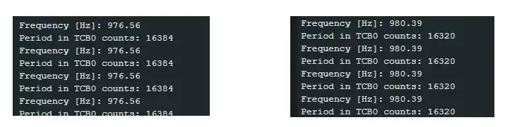
The result when using the megaAVR board package was 16384. analogWrite() is controlled via the Timer A clock, which uses the divider 64. Regardless of the duty cycle, rising and a falling edges are generated every 256 counter increments. The PWM signal therefore has a frequency of 16 MHz / (64 * 256) = 976.5626 Hz, or a period of 0.001024 seconds. The clock of Timer B corresponds to the system clock. This means that 16384 counter increments correspond to a frequency of 16 MHz / 16384 = 976.5625 Hz. So it fits perfectly!
With the MegaCoreX I determined a period of 16320 (= ~980.4 Hz), which surprised me at first. The reaon is: the analogWrite() function of the MegaCoreX package comprises only 255 steps: 16 MHz / (64 * 255) = ~980 Hz. This actually makes more sense than 256 steps, as analogWrite(pin, 255) provides a duty cycle of 100%. With the Arduino board package, analogWrite(pin, 255) generates a duty cycle of 255/256 * 100%, i.e. 100% cannot be achieved.
Input Capture Frequency Measurement Mode
The Input Capture Frequency Measurement Mode basically does the same as the Input Capture On Event Mode, except that the counter is reset to 0 after the event signal has been received. This has the advantage that CCMP provides us with the period directly, and we do not have to calculate differences.
The term “frequency measurement” is actually incorrect. It should be called “period measurement”.
ISR(TCB0_INT_vect){
    TCB0.INTFLAGS = TCB_CAPT_bm; /* Clear the interrupt flag */
}

void setup() {
    Serial.begin(115200);
    analogWrite(10, 192); // the event source
    EVSYS.CHANNEL1 = EVSYS_GENERATOR_PORT1_PIN1_gc; // PB1 (Pin 10) is event generator
    EVSYS.USERTCB0 = EVSYS_CHANNEL_CHANNEL1_gc; // TCB0 is event user
    TCB0.CTRLA = 0;
    TCB0.CTRLB = TCB_CNTMODE_FRQ_gc; // enable input capture frequency mode
    TCB0.EVCTRL = TCB_EDGE_bm | TCB_CAPTEI_bm; // enable capture event input
    TCB0.INTCTRL = TCB_CAPT_bm;  // enable capture event input
    TCB0.CTRLA = TCB_CLKSEL_CLKDIV1_gc | TCB_ENABLE_bm; // use system clock, enable TCB0

}

void loop(){
    Serial.print("Period in TCB0 counts: ");
    Serial.println(TCB0.CCMP + 1);
    float frq = 16000000.0 / ((TCB0.CCMP + 1) * 1.0);
    Serial.print("Frequency [Hz]: ");
    Serial.println(frq);
    delay(1000);
}
In this example sketch, I have integrated the calculation of the frequency into the sketch. It is interesting to note that you have to add 1 to the CCMP value to get the correct result. A CCMP value of 16383 is 16384 steps – that actually makes sense. The only thing that hasn’t really become clear, at least to me, is why you don’t have to add 1 when using the Input Capture On Event Mode.
Input Capture Pulse-Width Measurement Mode
The Input Capture Pulse-Width Measurement Mode allows you to measure the pulse width of signals. In contrast to Frequency Measurement Mode, in which only the rising or falling edge had an effect, in this mode the counter is “zeroed” on one edge and the input capture, i.e. writing the counter reading to CCMP, takes place on the other edge.
ISR(TCB0_INT_vect){
    TCB0.INTFLAGS = TCB_CAPT_bm; /* Clear the interrupt flag */
}

void setup() {
    Serial.begin(115200);
    analogWrite(10, 192); // the event source
    EVSYS.CHANNEL1 = EVSYS_GENERATOR_PORT1_PIN1_gc; // PB1 (Pin 10) is event generator
    EVSYS.USERTCB0 = EVSYS_CHANNEL_CHANNEL1_gc;  // TCB0 is event user
    TCB0.CTRLA = 0;
    TCB0.CTRLB = TCB_CNTMODE_PW_gc; // enable pulse width measurement mode
    TCB0.EVCTRL = TCB_CAPTEI_bm; // enable capture event input
    TCB0.INTCTRL = TCB_CAPT_bm;
    TCB0.CTRLA = TCB_CLKSEL_CLKDIV1_gc | TCB_ENABLE_bm; // use system clock, enable TCB0
    delay(10);
}

void loop(){
    Serial.print("High Period in TCB0 counts: ");
    unsigned int highCnt = (TCB0.CCMP + 1);
    Serial.println(highCnt);
    float pw = (highCnt * 1.0) / 16.0;  // cnt divided by 16 MHz
    Serial.print("Pulse width [µs]: ");
    Serial.println(pw);
    Serial.println();
    delay(1000);
}
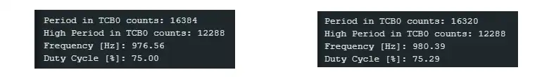
As a result, I received both the megaAVR package and MegaCoreX:

This corresponds exactly to expectations. The PWM period was 16384 counters long (megaAVR package). 75% of these are 12288. With MegaCoreX the period was 16320. 16320 / 255 * 192 = 12288 → this also fits well.
If you set the EDGE bit in the event control register (line 12), the sketch evaluates the LOW phase.
Input Capture Frequency and Pulse-Width Measurement Mode
The Input Capture Frequency and Pulse-Width Measurement Mode combines frequency and pulse-width measurement. Of course, not both values can be saved in CCMP. Instead, the mode works as follows (if the EDGE bit is not set):
- At first positive edge (pulse begins): The counter is reset and starts.
- Next negative edge (pulse ends): Input capture, i.e. the counter reading is written to CCMP.
- Second positive edge (period ends): Counter stops, an interrupt is triggered.
Since we know the period (from CCMP) and the pulse width (counter status at interrupt), we can calculate the duty cycle. And that’s precisely what the next sketch does:
volatile unsigned int period = 0;

ISR(TCB0_INT_vect){
    period = TCB0.CNT + 1; // Read the period
    TCB0.INTFLAGS = TCB_CAPT_bm; /* Clear the interrupt flag */
}

void setup() {
    Serial.begin(115200);
    analogWrite(10, 192);
    EVSYS.CHANNEL1 = EVSYS_GENERATOR_PORT1_PIN1_gc;
    EVSYS.USERTCB0 = EVSYS_CHANNEL_CHANNEL1_gc;
    TCB0.CTRLA = 0;
    TCB0.CTRLB = TCB_CNTMODE_FRQPW_gc;
    TCB0.EVCTRL = TCB_CAPTEI_bm; // TCB_EDGE_bm | TCB_CAPTEI_bm;
    TCB0.INTCTRL = TCB_CAPT_bm;
    TCB0.CTRLA = TCB_CLKSEL_CLKDIV1_gc | TCB_ENABLE_bm; // use system clock, enable TCB0
}

void loop(){
    Serial.print("Period in TCB0 counts: ");
    Serial.println(period);
    Serial.print("High Period in TCB0 counts: ");
    Serial.println(TCB0.CCMP + 1);
    float frq = 16000000.0 / (period * 1.0);
    Serial.print("Frequency [Hz]: ");
    Serial.println(frq);
    float dc = (TCB0.CCMP + 1) * 1.0 / (period * 1.0) * 100.0;
    Serial.print("Duty Cycle [%]: ");
    Serial.println(dc);
    Serial.println();
    delay(1000);
Here is the result:
Real-Time Counter – RTC Module
The RTC module offers two functions, namely the 16-bit Real-Time Counter (RTC) and the Periodic Interrupt Timer (PIT). Both use the same clock source. Otherwise, the functions can be used independently of each other. The maximum clock rate is 32768 Hz, so you are more likely to control the slower processes with this module.
The Registers of the RTC Module
Clock Selection Register CLKSEL

The clock is set in the CLKSEL register. The following options are available:
- INT32K_gc: 32768 Hz provided by the internal ultra low-power oscillator OSCULP32K.
- INT1K_gc: Like INT32K, but with a divider of 32, i.e. 1024 Hz.
- TOSC32K_gc: 32768 Hz through XOSC32K or an external clock at TOSC1.
- EXTCLK_gc: External clock generator connected to EXTCLK.
Crystal Frequency Calibration Register CALIB
A really great feature of the RTC module is that you can calibrate the underlying clock using the CALIB register.

ERROR[6:0] is the deviation in ppm. If SIGN is set, the clock is correspondingly faster. In this case, you must set the prescaler to at least DIV2. If SIGN is not set, the clock is slower.
RTC Control Register A CTRLA
In the CTRLA register, you specify whether the RTC module should continue to run in standby mode (RUNSTDBY). Furthermore, you (de)activate the calibration (CORREN) and enable the module (RTCEN).

You can use the PRESCALER to slow down the RTC with a maximum factor of 32768:
![PRESCALER[3:0] Bit Group Configurations](https://wolles-elektronikkiste.de/wp-content/uploads/2023/11/Reg_RTC_DIV_table-1024x381.webp)
RTC Interrupt Control Register INTCTRL
A Compare Match and an Overflow Interrupt are available for the RTC. The corresponding Interrupt Flag Register INTFLAG is similar.

PIT Control Register A CTRLA
The Periodic Interrupt Timer simply does what its name suggests: It triggers an interrupt at regular intervals. In the PITCTRLA register, you can activate the PIT and set the period.

![PERIOD[3:0] Bit Group Configurations](https://wolles-elektronikkiste.de/wp-content/uploads/2023/11/Reg_RTC_CYCLE_table.webp)
PIT Interrupt Control Register PITINTCTRL
In PITINTCRTL you activate the PIT interrupt. PITINTFLAGS is similar to PITINTCTRL.

Example Sketches for RTC and PIT
RTC example sketch
As a simple example for programming the RTC, here is a sketch that generates a “slow motion PWM” with a period of 2 seconds and a duty cycle of 75% at PE2 (= D13 = board LED).
ISR(RTC_CNT_vect){
    if(RTC.INTFLAGS & RTC_CMP_bm){ // check for CMP interrupt
        RTC.INTFLAGS = RTC_CMP_bm; // delete CMP interrupt flag
        PORTE.OUTCLR = PIN2_bm; // PE2 = LOW
    }
    if(RTC.INTFLAGS & RTC_OVF_bm){ // check for OVF interrupt
        RTC.INTFLAGS = RTC_OVF_bm; // delete OVF interrupt flag
        PORTE.OUTSET = PIN2_bm;  // PE2 = HIGH
    }
}

void setup() {
    delay(1);
    PORTE.DIRSET = PIN2_bm;
    RTC.CLKSEL = RTC_CLKSEL_INT32K_gc; // set internal clock @ 32768 Hz
    RTC.PER = 16383;  // TOP = 16383
    RTC.CMP = 12288;  // Compare value = 12288
    RTC.INTCTRL = RTC_CMP_bm | RTC_OVF_bm;  // enable CMP and OVF interrupts
    RTC.CTRLA = RTC_PRESCALER_DIV4_gc | RTC_RTCEN_bm; // Prescaler = 4 and enable RTC
}

void loop(){}
As only one interrupt vector (RTC_CNT_vect) is available for the Overflow and Compare Interrupt, we have to use the interrupt flags to check which event triggered the interrupt.
The prescaler is set to 4, i.e. the RTC counts at a frequency of 32768 / 4 = 8192 Hz. PER is 16383 and therefore the RTC overflows every 16384 steps, which corresponds to an overflow frequency of 2 seconds. The Compare Value is 12288, i.e. 75% of PER +1.
PIT example sketch
The example sketch for the PIT is even simpler. With a period of 16384 and a clock rate of 32768 Hz, an interrupt is triggered every 0.5 seconds. We use it in this sketch to toggle the board LED.
ISR(RTC_PIT_vect){
    RTC.PITINTFLAGS = RTC_PI_bm; // clear PIT interrupt flag
    PORTE.OUTTGL = PIN2_bm; // toggle PE2
}

void setup() {
    PORTE.DIRSET = PIN2_bm;
    RTC.CLKSEL = RTC_CLKSEL_INT32K_gc; // set internal clock @ 32768 Hz
    RTC.PITINTCTRL = RTC_PI_bm;  // enable PIT interrupt
    RTC.PITCTRLA = RTC_PERIOD_CYC16384_gc | RTC_PITEN_bm; // interrupt frq: 2 Hz
}

void loop(){}
A/D Converter – ADCn Module
The ADC of the Arduino Nano Every / “Nano 4808” would actually be worth its own article. However, I will keep this chapter short and ask you to look into the data sheet for further information. Here is the register summary:

I will go into a few selected register settings:
- RUNSTBY: Allows the ADC to be operated in standby mode.
- RESSEL: If you set this bit, the resolution is reduced from 10 to 8 bits.
- FREERUN: Continuous mode.
- SAMPNUM: You can add up to 64 results per measurement. 2^6 results times 2^10 resolution gives a result with a size of 2^16 bits, which still fits into the RES result register.
- PRESC: Divider for the clock rate of the ADC.
- REFSEL: Selection of the reference voltage. You can choose between: INTREF (Internal Reference), VDDREF and VREFA (External Reference). The data sheet incorrectly states “INTERNAL” and “VDD” instead of INTREF or VDDREF.
- COLLECT: Extends the measuring time up to a maximum factor of 31.
- MUXPOS: Defines the input for the ADC. The table with the bit group configurations can be found in the data sheet.
- STARTCONV: Starts a measurement.
The internal reference is specified in the VREF.CTRLA register. To do this, set the bit group ADC0REFSEL[2:0]. The available Bit Group Configurations are VREF_ADC0REFSEL_xxx_gc with xxx = 0V55, 1V1, 2V5V, 4V34 V or 1V5 for 0.55, 1.1, 2.5, 4.34 or 1.5 volts.
Example Sketches for the ADC
Simple ADC measurement
With the following example sketch, we measure the voltage at A2. We use the internal 4.34 V reference voltage.
void setup() {
    Serial.begin(115200);
    PORTD.PIN2CTRL = PORT_ISC_INPUT_DISABLE_gc; // Disable digital buffer
    ADC0.CTRLA = ADC_ENABLE_bm; // Enable ADC
    ADC0.CTRLC = ADC_REFSEL_INTREF_gc | ADC_PRESC_DIV16_gc; // use internal reference / prescaler: 16
    VREF.CTRLA = VREF_ADC0REFSEL_4V34_gc; // use internal 4.34 V reference
    ADC0.MUXPOS = ADC_MUXPOS_AIN1_gc; // use A2 (PD1) as input
    ADC0.SAMPCTRL = 0;
}

void loop(){
    ADC0.COMMAND = ADC_STCONV_bm; // Start Conversion
    while((ADC0.INTFLAGS & ADC_RESRDY_bm) == 0){} // Waiting for the result
    float res = ADC0.RES * 4340.0 / 1024.0;
    Serial.println(res);
    delay(1000);
}
ADC0 – RTC controlled
Let me come back to the events. The following sketch uses the RTC to initiate an ADC conversion every two seconds.
volatile bool adcReady = false;

ISR(ADC0_RESRDY_vect){
    adcReady=true;
}

void setup() {
    Serial.begin(115200);
    PORTD.PIN2CTRL = PORT_ISC_INPUT_DISABLE_gc;
    ADC0.CTRLA = ADC_ENABLE_bm;
    ADC0.CTRLC = ADC_SAMPCAP_bm | ADC_REFSEL_INTREF_gc | ADC_PRESC_DIV16_gc;
    VREF.CTRLA = VREF_ADC0REFSEL_4V34_gc;
    ADC0.MUXPOS = ADC_MUXPOS_AIN1_gc; // A2 (PD1)
    ADC0.SAMPCTRL = 0;
    ADC0.EVCTRL = ADC_STARTEI_bm; // initiate measurement by event
    ADC0.INTCTRL = ADC_RESRDY_bm; // enable result ready interrupt
    RTC.CLKSEL |= RTC_CLKSEL_INT32K_gc; // use internal 32 kHz clock
    RTC.PER = 63; // overflow after 63 (64 steps)
    RTC.CTRLA = RTC_PRESCALER_DIV1024_gc | RTC_RTCEN_bm; // OVF frequency = 0.5 Hz

    EVSYS.CHANNEL0 = EVSYS_GENERATOR_RTC_OVF_gc; // RTC overflow is event generator
    EVSYS.USERADC0 = EVSYS_CHANNEL_CHANNEL0_gc; // ADC0 is event user
}

void loop(){
    if(adcReady){
        float res = ADC0.RES * 4340L / 1024.0;
        Serial.println(res);
        adcReady = false;
    }
}
Without the event system, you would have to set up a timer interrupt or apply a construction with delay() or millis() to start measurements at 2-second intervals. You would then have to wait or be informed via another interrupt when the conversion result is available. In the example above, however, a single interrupt is sufficient, everything else is done in the background.
Watchdog Timer – WDT Module
The registers of the WDT Module
Two features in particular distinguish the WDT of the ATmega4808/4809 from the Arduino Nano Every and “Nano 4808”:
- The WDT has no interrupt.
- A WDT timeout always triggers a reset
The Watchdog Timer (WDT) receives its clock from the ultra low-power oscillator, OSCULP32K.
Control A Register CTRLA
You enter the timing parameters for the WDT in control register A, CTRLA.

You can make the following settings for PERIOD and WINDOW:
![WINDOW[3:0] / PERIOD[3:0] Bit Group Configurations](https://wolles-elektronikkiste.de/wp-content/uploads/2023/11/wdt_ctrla_settings-1024x404.webp)
If you only set a value for PERIOD and keep WINDOW at 0, the WDT will run in Normal Mode. If no watchdog reset takes place within the time period defined with PERIOD, a system reset is carried out.
If WINDOW is not zero, you are in Window Mode. This is a little more difficult to explain, and perhaps only becomes clear with the example sketch. The following applies in window mode:
- After initialization or a
wdt_reset(), the WDT is in the period defined by WINDOW. The data sheet calls this period “closed window time-out period” (TOWDTW). The WDT cannot be reset during this period. Awdt_reset()within this period leads to an immediate system reset. - After the TOWDTW, the “normal window time-out period” (TOWDT) begins, the length of which you specify with PERIOD. If a
wdt_reset()is received during this time, the game starts again from the beginning with the TOWDTW. - If there is no
wdt_reset()in the TOWDTW + TOWDT period, a system reset is carried out.
Status Register STATUS

By setting the LOCK bit, you protect the WDT settings against changes. You can only delete it again in debug mode.
If you write data to the CTRLA register, it must be transferred to the WDT clock domain. The SYNCBUSY bit is set during synchronization.
Example Sketch for the WDT
The Normal Mode should not require a sample sketch. That’s why we’re only looking at one sketch for the Window Mode. The setting for the WDT is: TOWDTW = TOWDT = 4 seconds.
#include <avr/wdt.h>
void setup(){
    Serial.begin(115200);
    Serial.println("*******************");
    Serial.println("Watchdog Timer Test");
    Serial.println("Sketch starts...");
    CPU_CCP = CCP_IOREG_gc; // allow changes
    WDT.CTRLA = WDT_WINDOW_4KCLK_gc | WDT_PERIOD_4KCLK_gc; // 4s period and window
    CPU_CCP = CCP_IOREG_gc;
    WDT.STATUS = WDT_LOCK_bm;
    while(WDT.STATUS & WDT_SYNCBUSY_bm){} // wait until WDT is synchronized
    wdt_reset();
    int seconds = 0;
    while(seconds < 100){
        // if(seconds == 5){  // try also 3
        //     wdt_reset();
        // }
        Serial.print(seconds);
        Serial.println(" seconds");
        delay(1000);
        seconds++;
    }
}

void loop(){}
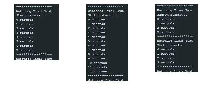
If you let the sketch run unchanged, the while() loop counts up until TOWDTW + TOWDT = 8 seconds have passed. The last output is “7 seconds” because once the eighth second has been reached, there is no more time for the output of “8 seconds”.
If you uncomment lines 15 to 17, there is a wdt_reset() at fifth second, i.e. in the “allowed” TOWDT period. The WDT then runs for a further eight seconds until the system reset is carried out.
If you then change line 15 so that the wdt_reset() occurs after three seconds, there will be an immediate system reset as you are in the “forbidden” TOWDTW period.
And what’s the point of all this? The watchdog normally bites if the sketch gets stuck somewhere. You can use the Window method to reset the system if an action is executed too early, for example because some other step was not executed for whatever reason.
Configurable Custom Logic – CCL Module
With the Configurable Custom Logic Module CCL, the Arduino Nano Every or “Nano4808” gains capabilities for which you would otherwise have to use external logic ICs. But it goes far beyond that.
The CCL module is organized in four so-called Look-Up Tables (LUTs). Each LUT has three inputs and one output.
In my pinout diagrams, I have labeled the inputs as x-INy, with x = 0 to 4 (number of the LUT) and y = 0 to 2. The outputs are labeled x-OUT with x = 0 to 3.
Register of the CCL Module
I will only give a rough overview of this module. Here is the register overview:

Each LUT has its own TRUTH register. This is where you define which input level combination is true. Example: For LUT2, we define that 2-IN2 = HIGH, 2-IN1 = LOW and 2-IN0 = LOW should be the “true” state. I.e: HIGH/LOW/LOW ⇒ 0b100 = 4. This in turn means that bit no. 4 must be set in TRUTH2 (and not that TRUTH2 = 4!).
Now comes the ingenious part: The inputs do not have to be just I/O pins, but can also be events, timers, USARTs or the output of another LUT, for example. So if certain states of different modules in your program require an action, you can save yourself the trouble of querying these states and some if and switch combinations with the CCL. You define the inputs via the Input Select Bitgroups (INSELn[3:0]).
If the “true” state occurs, you can be notified by an interrupt. Alternatively or additionally, you can set the OUTEN bit so that the corresponding output goes from LOW to HIGH when “true”.
You can even combine 2 LUTs (LUT0 and LUT1 or LUT2 and LUT3) using the SEQSELn[3:0] bit groups.
Example Sketch for the CCL Module
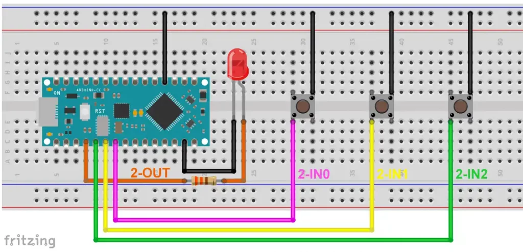
As a simple example, we check the status of the I/O pins assigned to LUT2. The following applies to the Arduino Nano Every:
- 2-IN2 = PD2 = A1
- 2-IN1 = PD1 = A2
- 2-IN0 = PD0 = A3
- 2-OUT = PD3 = A0
Our true condition should be: 2-IN2 = HIGH, 2-IN1 = LOW and 2-IN0 = LOW. We pull the inputs to HIGH with the internal pull-up resistors. Pressing the button should bring them to LOW. If the buttons on 2-IN1 and 2-IN0 are pressed, the true condition is fulfilled and output 2-OUT goes HIGH. This is indicated by an LED. This is the circuit:
And here is the corresponding sketch:
void setup() {
    PORTD.DIRCLR = PIN2_bm | PIN1_bm | PIN0_bm; // PD0 = A3 = 2-IN0 as input, etc.
    PORTD.PIN0CTRL = PORT_PULLUPEN_bm; // PULLUP for PD0 = A3 = 2-IN0
    PORTD.PIN1CTRL = PORT_PULLUPEN_bm; // PULLUP for PD1 = A2 = 2-IN1
    PORTD.PIN2CTRL = PORT_PULLUPEN_bm; // PULLUP for PD2 = A1 = 2-IN2
    CCL.LUT2CTRLB = CCL_INSEL0_IO_gc | CCL_INSEL1_IO_gc; // select I/O as input
    CCL.LUT2CTRLC = CCL_INSEL2_IO_gc; // select I/O as Input
    CCL.TRUTH2 = 0x10; // 2-IN2 = HIGH, 1-IN2 = LOW, 0-IN2 = LOW ==> TRUE
    CCL.LUT2CTRLA = CCL_OUTEN_bm | CCL_ENABLE_bm; // OUT Enable / LUT2 enable
    CCL.CTRLA = CCL_ENABLE_bm; // CCL_ENABLE
}

void loop(){}
The MegaCoreX board package has implemented its own library called Logic for the CCL module.
The Arduino Nano Every goes to sleep – SLPCTRL Module
Going to sleep – I think this is a good topic for the last chapter!
Register Settings for SLPCTRL
The SLPCTRL module only has the CTRLA register, in which you select the sleep mode (SMODE[1:0]) and enable the SLPCTRL module using the SEN bit. However, setting the SEN bit alone does not put the microcontroller to sleep. To do this, use sleep_cpu() from avr/sleep.h.

You can select from the following options for Bit Group Configurations for SMODE[1:0]:
- IDLE: Idle – the lightest sleep; everything is active except the CPU.
- STANDBY: Stand-by – the most flexible setting.
- PDOWN: Power Down – deep sleep.
The deeper the sleep, the lower the power consumption and the more limited the wake-up methods. Which peripherals are available in which sleep mode can be found in the data sheet, chapter 11.3.2.1. Stand-by mode is the most flexible. Many modules have a RUNSTBY bit that determines whether the module should be available in standby mode or not.
Example sketch for SLPCTRL
In the following example, we bring the Arduino Nano Every / “Nano4808” in Power Down Mode and wake it up after one second using the Periodic Timer Interrupt (PIT).
 #include<avr/sleep.h>

ISR(RTC_PIT_vect){
    RTC.PITINTFLAGS = 1;
}

void setup(){
    Serial.begin(115200);
    RTC.CLKSEL = RTC_CLKSEL_INT32K_gc;
    RTC.PITCTRLA = RTC_PERIOD_CYC32768_gc | RTC_PITEN_bm;
    RTC.PITINTCTRL = RTC_PI_bm;
    SLPCTRL.CTRLA = SLPCTRL_SMODE_PDOWN_gc | SLPCTRL_SEN_bm;
}

void loop(){
    Serial.println("Going to sleep...");
    Serial.flush();
    sleep_cpu();
}
In the sleep example the include file is not needed
#include
The line
sleep_cpu();
can be replaced by
asm(“sleep”);
Thank you very much for your excellent insight, Herr Ewald.
Such clearly and comprehensive information is quite hard to find in the Arduino world, even from the official site.
I just wanted to comment about the use of Timer B in the nano Every.
You indicate:
“Timer B – TCBn Module
The Arduino Nano Every, or the ATmega4809 on which it is based, has four 16-bit Timers B (TCB0 to TCB3). The “Nano 4808” has three of these timers (TCB0 to TCB2). …
For time measurements (millis(), delay()) the board packages use the TCB3 (Arduino Nano Every) …”
I have an application that implements Timer A and also measurements with millis(). I was receiving incorrect millis() reports until I disabled Timer A. Then millis() measurements were correct.
I wonder if a setting of Timer A can also influence millis(). I have read the Atmega4809 datasheet in some detail, but timers are quite complex peripherals and didn’t find a clear explanation.
The official Arduino site says this about millis():
“Reconfiguration of the microcontroller’s timers may result in inaccurate millis() readings. The “Arduino AVR Boards” and “Arduino megaAVR Boards” cores use Timer0 to generate millis().”
I understand that they are actually talking of Timer A in case of megaAVR Boards, like the Nano Every.
I would appreciate your comments.
Best regards,
Hi, Timer A and Timer B are not completely independent when using the megaAVR board package. The package sets the divider of Timer A to 64 and uses the Timer A clock for Timer B. You should therefore not change the divider. Could it be that you have changed the Timer A divider? Maybe you try the MegaCoreX package?
Best regards, Wolfgang
I am finding your post on a Deep Dive into the Nano Every to be very helpful. Thank you for all the hard work!
I am still trying to find my way, but I did notice one difference between your Pinout diagram and another one that I had found earlier. You say that the SPI signal SS is on pin D10. The other source says it is on pin D8.
When I look here:
~\Arduino15\packages\arduino\hardware\megaavr\1.8.8\variants\nona4809\pins_arduino.h
I find the line “#define PIN_SPI_SS (8). I don’t have enough experience to know if that answers the question or not, but I thought you would like to know about it.
Again, thank you and best regards.
You are absolutely right! Thanks for informing me. I will soon upload a corrected image.