About this post
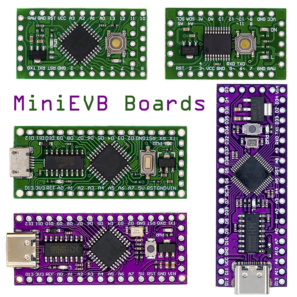
The MiniEVB boards differ mainly in the design of their underlying microcontroller LGT8F328P. In addition, there are different board layouts that are modeled after the Arduino Nano or Pro Mini. Both aspects determine which port pins and functions are available and via which board pins you can access them. And because this is a bit confusing, I’ve dedicated an entire post to the topic. Furthermore, I will discuss the power consumption of the different boards in awake and sleep mode.
How to program LGT8F328P boards and how they differ from ATmega328P based boards I described in my last post using the example of LQFP32 boards.
This post will cover the following topics:
- Overview
- LQFP48 MiniEVB (“Nano Style”)
- Conversion of the reset pin to an I/O pin (all MiniEVB boards)
- Using SWC and SWD as I/O pins (all MiniEVB boards)
- Setting up alternative output pins (all MiniEVB boards)
- Using OC3A as digital output pin (LQFP48 MiniEVB only)
- 80 mA output (all MiniEVB boards)
- Analog differential measurements (all Mini EVB boards)
- LGT8F328P LQFP32 MiniEVB (“Nano Style”)
- LGT8F328P LQFP32 MiniEVB, “Pro Mini Style”
- LGT8F328P SSOP20 MiniEVB, “Pro Mini Style”
- Power consumption
To control the MiniEVB boards, I use the great board package lgt8fx from David Buezas, as I did in the last post.
Overview
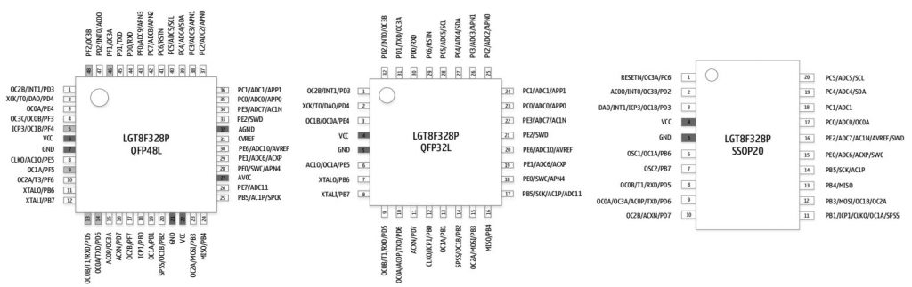
The LGT8F328P is available in QFP48L, QFP32L and SSOP20 packages (click on the image to enlarge):
Before we get further into the details, I want to define a few terms so that we are speaking the same language:
- Port pins are the port inputs/outputs, like PB0, PD7 etc.
- IC pins are the physically available pins of the LGT8F328P chip.
- Board Pins are the pins of the MiniEVB boards, which you access via the pin headers.
The term “port pin” is actually not ideal, since a port pin is not a pin in the true sense of the word. Better might be “GPIO” (General Purpose Input Output). However, this is rather unusual in the Arduino / AVR world. The most important thing is that you know what is meant.
The design of the underlying IC determines which port pins of the LGT8F328P are available as IC pins and which functions are assigned to them. Then it gets a little confusing:
- The QFPL32 has PD1 and PF1 assigned to the same IC pin (although this is not clear from the datasheet pinout diagram). The same applies to PD2 and PF2.
- The SSOP20 IC has even more double assigned IC pins, one is even triple assigned (PD3, PD4, PF4).
- On the MiniEVB boards, on the other hand, not all the IC pins are accessible via board pins.
The following table summarizes which port pins on the MiniEVBs are available as board pins, for which this is not the case and which share an IC or board pin.

The resulting number of pins is:
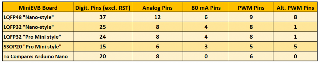
Notes on my counting method:
- Since the analog pins can be used as digital pins (exception: A6/A7 of the original Nano), I counted them as digital pins as well. So, this is the maximum number of digital pins available.
- IC pins which are available on multiple board pins, I have considered only once.
- Port pins that share a board pin were counted only once.
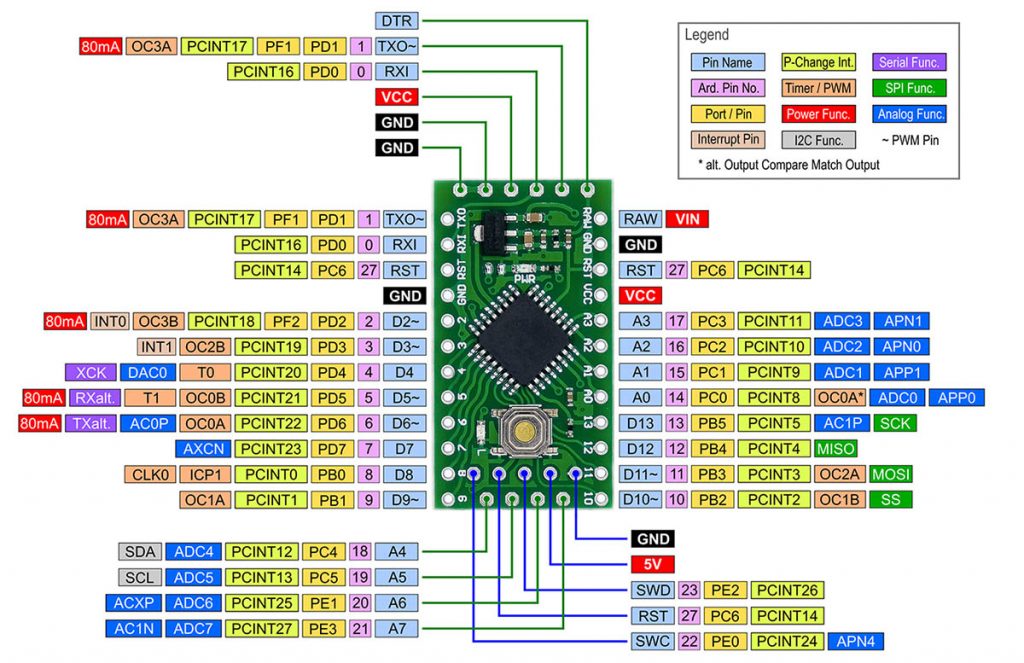
LQFP48 MiniEVB (“Nano Style”)
Now we take a detailed look at the boards and start with the “Nano Style” LQFP48 MiniEVB.
In comparison to the ATmega328P, the LGT8F328P has two additional ports (E and F) and the port pin PC7. This makes a total of 40 port pins, all of which are implemented on the QFP48L IC. PB6 and PB7 are used on the LQFP48 MiniEVB for the external oscillator. Therefore, they are inaccessible via board pins. PC6 is assigned the reset function, which leads to certain constraints for its use as I/O pin.
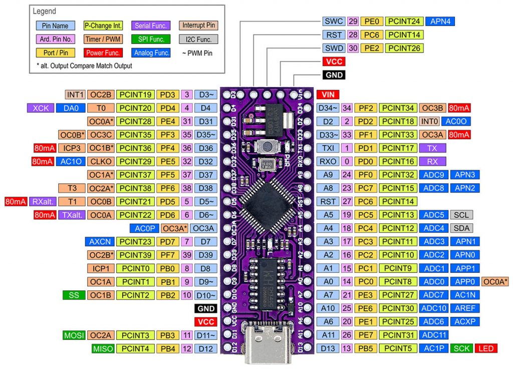
It is interesting to note that the QFP48L has a separate pin for the output compare match of Timer3, namely OC3A. Hence, you can use it for providing PWM signals without blocking any of the I/O pins. By programming Timer3 appropriately, OC3A can also be used as an additional digital output pin. We’ll get to that.
Conversion of the reset pin to an I/O pin (all MiniEVB boards)
If you run out of pins, you can easily convert the reset pin to an I/O pin. But only apply this if you know exactly what you are doing! The following must be considered:
- Once you have converted the reset pin to an I/O pin, you can only upload your sketches via LArduinoISP, or:
- You make PC6 the reset pin again by burning the bootloader. But for this, you have to go the detour via LArduinoISP again.
- The reset pin is configured as reset input during boot, regardless of your settings. I.e. even if you use it as I/O pin, you must not pull it to GND when booting. If you do so, the LGT8F328P will remain in reset mode.
If, despite these limitations, you still want to try to convert the reset pin, you could now attach an LED to the reset pin and upload the following sketch:
void setup(){
    PMX2 |= (1<<WCE); // change enable
    PMX2 |= (1<<C6EN); // enable PC6 (RST) as I/O Pin
    pinMode(28, OUTPUT); // RST = 28 for QFP48L, RST = 27 for QFP32L / SSOP20
}

void loop() {
    digitalWrite(28, HIGH);
    delay(200);
    digitalWrite(28, LOW);
    delay(200);
}
Line 2 sets the Change Enable Bit WCE in the I/O Reset Register PMX2. Only then can changes be made in the register. In line 3, bit C6EN is set, turning the reset pin into an I/O pin. It’s as simple as that.
Using SWC and SWD as I/O pins (all MiniEVB boards)
In addition, the SWC and SWD pins required for programming via LArduinoISP can be used as normal I/O pins. You do not need to make any special settings for this. However, there is one point to consider when uploading via LArduinoISP. This works so simply only once. If you have uploaded a sketch to the MiniEVB that uses SWD or SWC as a normal I/O pin, you will get an error message the next time you try to upload via LArduinoISP. Workaround: Press the reset button of the board to be programmed during the upload.
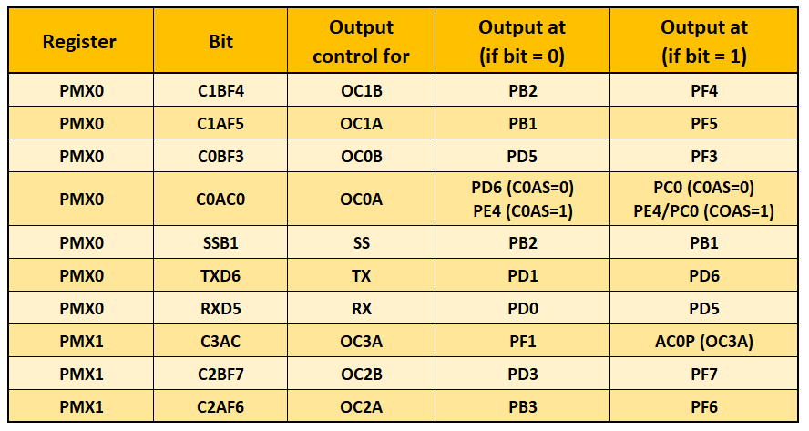
Setting up alternative output pins (all MiniEVB boards)
The LQFP48 MiniEVB board not only has many I/O pins, but many functions can be routed to alternate pins. This applies to RX, TX, SS and most PWM channels. I have marked the alternative PWM outputs with an asterisk in the pinout diagram.
To use the alternative outputs, you only have to set the Change Enable bit in PMX0 and then the bit responsible for the function in PMX0 or PMX1.
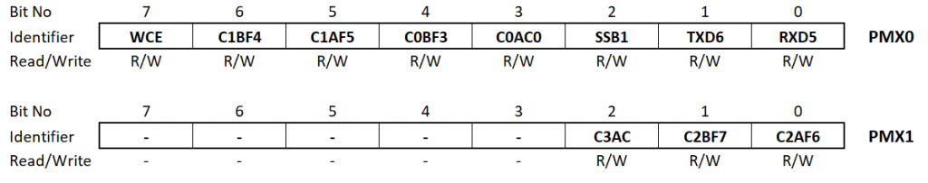
The following table gives an overview of the bits and their effect regarding the outputs:
An example
The following sketch generates a PWM signal at PB3 (D11) which is the default OC2A output. If you uncomment lines 5 to 7 and comment line 8, you will get the PWM signal at the alternative output PF6 (D38).
void setup(){
  noInterrupts();
  TCCR2A = (1<<COM2A0);
  TCCR2B = (1<<CS20);
//  PMX0 = (1<<WCE);
//  PMX1 = (1<<C2AF6);
//  DDRF = (1<<DDF6);
  DDRB = (1<<DDB3);
  OCR2A = 85;
  interrupts();
}
void loop(){}
OC0A Alternatives
OC0A is a special case because you can move the output from PD6 (D6) to PC0 (A0) or to PC0 (A0) and PE4 (D31). Here is an example of the output to PC0:
void setup(){
  noInterrupts();
  TCCR0A = (1<<COM0A0);
  TCCR0B = (1<<CS00); // Normal mode
  PMX0 = (1<<WCE);  // Change enable
  PMX0 = (1<<C0AC0);  // OC0A output at PC0 (= A0/14)
  DDRC = (1<<DDC0); // Set PC0 to output
  OCR0A = 85;
  interrupts();
}

void loop(){}
And this is what a sketch looks like for simultaneous output on both alternate pins:
void setup(){
  noInterrupts();
  TCCR0A = (1<<COM0A0);
  TCCR0B = (1<<OC0AS)| (1<<CS00);  // Normal Mode, Output at PE4 (31)
  PMX0 = (1<<WCE);  // Change enable
  PMX0 = (1<<C0AC0); // OC0A output at PC0 (= A0/14)
  DDRC = (1<<DDC0); // Set PC0 to output
  DDRE = (1<<DDE4); // Set PE4 to output
  OCR0A = 85;
  interrupts();
}

void loop(){}
The only difference: In the second sketch, the OC0A select bit OC0AS in the Timer Counter 0 Control Register B (TCCR0B) was additionally set and PE4 was set as output.
If you don’t feel like picking out all the bits and registers for PWM programming from tables, I recommend the Arduino Web Timers tool. This allows you to “click” together the timer and PWM settings from a selection and get the finished code. The tool works for the LGT8F328P as well as for the ATmega328P and ATmega328PB.
Using OC3A as digital output pin (LQFP48 MiniEVB only)
Sometimes it’s that one pin you’re missing to make your project happen. If this is the case for you, you can use OC3A like a digital output pin. To set it HIGH, generate a PWM signal with 100% duty cycle. For LOW, the duty cycle is correspondingly 0%. Here is a blink sketch for OC3A:
void setup(){
  noInterrupts();
  TCCR3A = (1<<COM3A1); // Clear OC3A on compare match
  TCCR3B = (1<<WGM32) | (1<<CS30); // Top = OCR3A / no prescaler
  PMX0 = (1<<WCE); // change enable
  PMX1 = (1<< C3AC); // Output at AC0P (OCR3A)
  OCR3A = 0; // OC3A will be cleared / set immediately
  interrupts();
}

void loop(){
    setOCR3A(HIGH);
    delay(500);
    setOCR3A(LOW);
    delay(500);
}

void setOCR3A(bool setOn){
    noInterrupts();
    if(setOn){
        TCCR3A = (1<<COM3A1) | (1<<COM3A0); // Set OC3A on compare match
    }
    else{
        TCCR3A = (1<<COM3A1); // Clear OC3A on compare match
    }
    interrupts();
}
80 mA output (all MiniEVB boards)
On the LQFP48 MiniEVB board, all six 80 mA outputs are available. The following sketch shows how to activate the 80 mA function using PF2 / pin 34 as an example:
/*
       HDR      Port/Pin     Arduino Pin
       HDR0       PD5            5
       HDR1       PD6            6
       HDR2       PF1           33
       HDR3       PF2           34
       HDR4       PE4           36
       HDR5       PF5           32
*/

void setup(){
/* example for activating PF2/34 for high current */
    HDR |= (1<<HDR3);
    pinMode(34, OUTPUT);
}

void loop(){
    digitalWrite(34, HIGH);
    delay(500);
    digitalWrite(34, LOW);
    delay(500);
}
But be especially careful here with the boards (which we’ll get to) that assign run two port pins on one IC pin – you could cause a short.
Analog differential measurements (all Mini EVB boards)
An advantage of the MiniEVB boards compared to the AVR based Arduinos is the possibility to perform differential measurements and to amplify the measured values. With the LQFP48 MiniEVB you can use the following pin combinations for differential measurements:
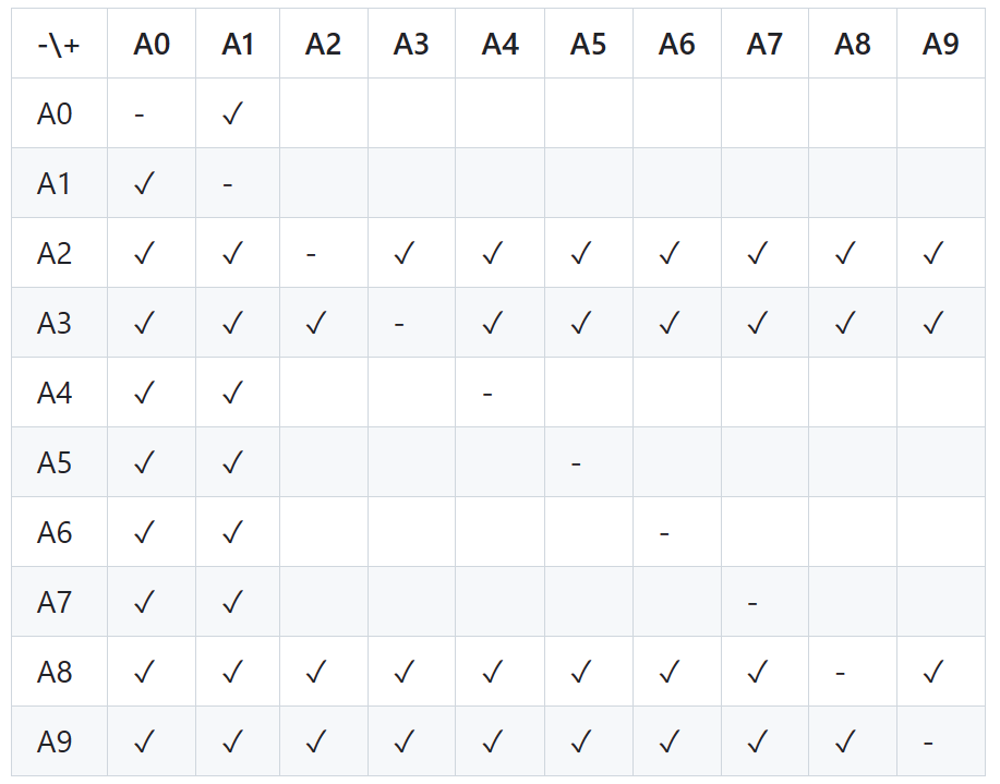
I took the graphic from the differential_amplifier library documentation(here). I have described how to use the library here, so I won’t repeat it in this post.
LGT8F328P LQFP32 MiniEVB (“Nano Style”)
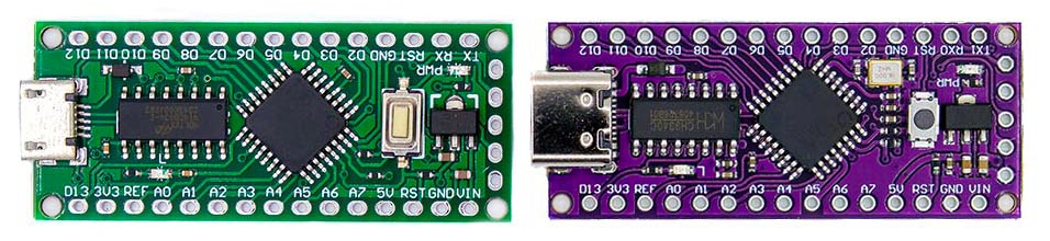
The “Nano Style” LQFP32 MiniEVB is currently available in two versions. The green board has a Micro-USB connector, has no external oscillator and uses the HT42B534-2 as USB-to-TTL chip. The purple board has a USB-C connector, a 16 MHz oscillator and it uses the CH9340C USB-to-TTL chip. Both variants have a similar pinout. The pin designations and their positions on the long sides correspond to those of the Arduino Nano.

Everything else follows from the pinout scheme. PF1 and PF2 are assigned to the same IC and Board pins as PD1 and PD2. This makes OC3A and OC3B accessible at D1 and D2. The rest of the PORTF pins are missing. For PORTE only 5 pins are available and for PORTC PC7 is not assigned to any board pin.
Despite its similarity to the Arduino Nano, the board has five additional digital inputs/outputs. AREF, A6 and A7 can be used as digital pins, plus the SWC and SWD.
Which is better – purple or green board?
Aside from color preferences, there are two technical aspects to consider from my perspective:
- The power consumption of the purple board is lower (at least when not powered by USB). I will come to this in detail further below.
- For time-critical applications, the external oscillator of the purple board is advantageous.
According to the data sheet, the internal oscillator of the LGT8F328P is calibrated to a maximum deviation of 1% (10000 ppm). I have not found more detailed information about the conditions, such as the temperature. For external oscillators, frequency stabilities in the range 10 – 100 ppm are specified. With 100 ppm deviation, a “millis()–clock” (see e.g. here) would theoretically deviate 8.6 seconds per day.
I did a practical test by using the purple board to test the deviation of a millis()-clock when using the internal and external oscillator. Result:
- internal: 0.42 % (363 seconds / day)
- external 0.05 % (43 seconds / day)
The external oscillator is more accurate, but the deviation is higher than the frequency stability would suggest. This is because the frequency stability only indicates how the frequency can deviate from a baseline under certain conditions over a certain period of time. It therefore does not indicate the absolute deviation, which depends on other parameters.
I have performed the measurements only once. So take the results as a one-time empirical value.
The purple board has one disadvantage, and that is that it can not be used as an LArduinoISP programmer for reasons that are not yet clear to me.
LGT8F328P LQFP32 MiniEVB, “Pro Mini Style”
The LGT8F328 LQFP32 MiniEVB in “Pro Mini Style” differs from its “Nano Style” counterpart in several aspects:
- The position of the board pins is different.
- The USB-to-TTL adapter is missing.
- PE6 (AREF) is not connected to any board pin.
- The board is available with either a 5V or a 3.3V voltage regulator.
- This can be very helpful for controlling 3.3V devices.
It is a mystery to me why the designers of the “Pro Mini Style” LQFP32 MiniEVB did not assign AREF to any board pin. Probably, they wanted to get as close as possible to the original Arduino Pro Mini. But there would have been potential for improvement here. The triple assignment of the reset pin or the fivefold (!) assignment of GND could have been omitted for this. If you are skilled, you can solder a connector directly to the pin 20 of the LGT8F328P. But actually, you buy boards not to do this kind of soldering.
LGT8F328P SSOP20 MiniEVB, “Pro Mini Style”
The SSOP20 “Pro Mini Style” MiniEVB is a very peculiar board, mainly due to the type of LGT8F328P IC on which it is based. Many port pins are not implemented and some port pins share a board pin.

The following sketch flashes an LED connected to pin 3/4 using the underlying port pins PD3, PD4 and PF4. It should be noted that in such a case of double or triple assignment, one should never set one of the affected port pins to OUTPUT / HIGH while the other(s) are set to OUTPUT / LOW. The result is a short circuit. At best, only the LED remains dark.
void setup(){}

void loop(){
    DDRD = (1<<DDD3);
    PORTD |= (1<<PD3);
    delay(200);
    PORTD &= ~(1<<PD3);
    delay(200);

    DDRD = (1<<DDD4);
    PORTD |= (1<<PD4);
    delay(200);
    PORTD &= ~(1<<PD4);
    delay(200);
    DDRD = 0;

    DDRF = (1<<DDF4);
    PORTF |= (1<<PF4);
    delay(200);
    PORTF &= ~(1<<PF4);
    delay(200);
    DDRF = 0;

    delay(2000);
}
Personally, I see no reason why you should use the SSOP20 MiniEVB “Pro Mini Style” board. If you want to use a board in “Pro Mini” design, my choice would always be the LQFP32 variant. The size difference is also small. The SSOP20 version is only one pin shorter, i.e. 2.54 millimeters.
Power consumption
Power consumption in awake mode
To measure power consumption in awake mode, I first loaded the following sketch onto the boards to be tested:
void setup() {}

void loop() {
  delay(10000);
}
In the Arduino IDE, I chose the board type and varied the frequency using the clock divider. Then I disconnected the board from the PC, connected it to a power supply instead, and measured the current.
There are three options for power supply without a computer:
- With a plug via the USB port (if available on the board).
- Disadvantage: The protection diode on the board reduces the voltage by approx. 0.3 volts.
- Advantage: Reverse polarity protection.
- Via VIN or RAW (designation varies).
- Disadvantage: higher voltages needed (min. 6.5 volts).
- Advantage: stable supply with 5 volts, as long as the voltage source is min. 6.5 volts.
- Via VCC or 5V (designation varies).
- Disadvantage: In battery operation, the operating voltage changes with the state of charge
- Advantage: Power supply < 5 V possible, e.g. operation with Li-Ion battery.
Since I wanted to check the influence of the operating voltage on the power consumption, I chose option 3. 5 volts or 3 volts were used as the operating voltage.

Besides the LGT8F328P, the LEDs, the voltage regulator (although operated “from behind”) and the USB-to-TTL adapter also consume power. To determine this influence, I took an LQFP32 “Pro Mini” and removed only the LEDs or the LEDs and the voltage regulator.
Results
Some of the results were quite surprising:
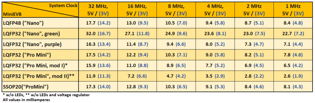
Conclusions:
- You can significantly reduce the power consumption by lowering the clock rate.
- Lowering the operating voltage from 5 volts to 3 volts will save 3 to 4 milliamperes on the (unmodified) boards. One exception is the green LQFP32 “Nano Style”, more about this below.
- The board LED consumes approx. 1.3 milliamps at 5 volts at 5 volts and 0.6 milliamps at 3 volts.
- The voltage regulator “eats” about 4 milliamps at 5 volts, and about 2.3 milliamps at 3 volts.
- The savings by lowering the operating voltage are mainly due to the LEDs and the voltage regulator.
For comparison, an Arduino Nano (16 MHz / 5 V) based on the ATmega328P / CH340G consumed 22.3 milliamps in my tests.
How to reduce the power consumption of the green LQFP32 “Nano Style” board
The high current consumption of the green LQFP32 “Nano Style” board at 5 volts stands out, as does the saving of about 15.5 milliamperes when lowering the operating voltage to 3 volts. These phenomena are related to the USB-to-TTL chip HT42B534 (datasheet here). Actually, the HT42B534 should go in power saving mode when USB is disconnected, but it obviously doesn’t, at least at 5 V power supply. The CH9340C on the purple board does a better job.

However, the problem is not the HT42B534 itself, but how it is wired on the board. The good news: there is a remedy. If you pull the “D-” input (physical pin 2) to LOW at least at power-up, the HT42B534 goes into sleep mode. There are several ways to achieve this.
If you have a steady hand, you can solder a pull-down resistor directly to the pins GND (No. 4) and “D-” (No. 2). Sketch uploads or communication with the serial monitor in normal USB operation are not disturbed by this. With a 10 kΩ resistor this worked fine for me.
If you don’t like this, you can also connect “D-” to GND using the following tools:
- USB Breakout Board + Micro-USB to Micro-USB cable
- Adapter for Micro-USB to screw terminal
- USB connector for soldering
It might be interesting to note that even without such measures, the power consumption only goes up to about 22 milliamps if you start the board with three volts and then increase the voltage to five volts. I do not have an explanation for this, to be honest.
But these are all stopgap solutions. If you want to use a LQFP32 LGT8F328P in battery-powered projects, then better go for the purple board, the “Pro Mini Style” version or take the bare LQFP32 IC. For the latter, I paid €1.36 plus 60 euro cents for an adapter board. Soldering SMDs is not everyone’s favorite thing (I don’t like it much either), but it’s not as difficult as one might think.
Power consumption at operation via VIN / RAW
The power consumption of the MiniEVB boards was only slightly higher when supplied with 8 volts via VIN than when supplied with 5 volts via VCC. Checks with different boards and frequencies showed differences from 0.0 to 0.3 milliamperes.
Power consumption in sleep mode
Finally, let’s take a look at the power consumption in the different sleep modes. For this, I used the library lgt_LowPower from LaZsolt, which is part of the board package lgt8fx.
The sleep modes of the LGT8F328P are fundamentally different from those of the ATmega328P. However, to make life easier for the users, the lgt_LowPower library uses the same function names as you know them from the AVR world. For the details of the sleep modes, please check out the documentation on GitHub.
I used the following sketch to set the different sleep modes:
#include "lgt_LowPower.h"

void setup()
{
  // Pin settings for low consumption in sleep mode.
    DDRB  = 0x00;                 // Set all pins to input
    DDRC  = 0x00;
    DDRD  = 0x00;
    DDRE  = 0x00;
    PORTB = 0xFF;                 // Set all input with internal pull up resistors
    PORTC = 0xFF;
    PORTD = 0xFF;
    PORTE = 0xFF;
//    IOCWK = (1<<PORTD4);  // for deepSleep2 mode (level change wake up at D4)
}

void loop() {
    delay(15000); // To get stable power consumption in active mode

//    LowPower.idle(SLEEP_32S,ADC_OFF,TIMER3_OFF,TIMER2_OFF,TIMER1_OFF,TIMER0_OFF,
//    SPI_OFF,USART0_OFF,TWI_OFF,PCIC_OFF,FLASHCTL_OFF);

//    LowPower.adcNoiseReduction(SLEEP_32S, ADC_ON, TIMER2_OFF);

//    LowPower.powerStandby(SLEEP_FOREVER, ADC_OFF, BOD_OFF, TIMER2_OFF);

//    LowPower.powerExtStandby(SLEEP_FOREVER, ADC_OFF, BOD_OFF, TIMER2_OFF);

     LowPower.powerDown(SLEEP_FOREVER, ADC_OFF, BOD_OFF);

//    LowPower.deepSleep2(SLEEP_FOREVER);

}
My test objects were a LQFP32 MiniEVB board in “Pro Mini Style” and my LQFP32 based DIY board. Since the voltage regulator and the LEDs of the “Pro Mini Style” board are significant power consumers, the modified board, where I had removed these components, was used here again. The power supply with 5 volts was provided via VCC / GND.
Results
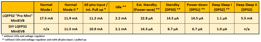
- LEDs and voltage regulator consume about 5.5 milliamps (see Normal Mode I vs. Normal Mode II and Deep Sleep I vs. Deep Sleep 2).
- Setting all pins to INPUT/HIGH (in
setup()) will save 0.6 – 0.7 milliamps. - In DPS2 mode, without LEDs and voltage regulator, the power consumption can be reduced to 1 microampere. For DPS2 mode, however, note:
- Waking up leads to a reboot.
- Program uploads to a board in DPS2 mode may fail. Workaround: Wake it up or reset it shortly before upload.
- Why the DIY (do-it-yourself) module consumes even less power than the “Pro Mini Style” board without LEDs and voltage regulator, I can’t say for sure.
Acknowledgement
Thanks to dbuezas for reviewing this post!
Hi Wolfgang, and thank you for your useful posts
I want to use internal 4.096V reference voltage for ADC of LGT8F328P SSOP20 board in my project. I’m using platform IO in VS Code for development. Based on my findings in web I should use “analogReference(INTERNAL4V096); ” function for that. but the result is ADC Ref Voltage sets to 1.024V.
I rummaged the “wiring_analog.c” and “pins_arduino.h” files in lgt8fx framework for PlatformIO discovered the following problem in “analogReference()” function definition: they used the macro definition checking (#if defined(__LGT8FX8P__)) for compile time. But because of __LGT8FX8P__ never defined, the section of code that contains correct voltage settings was skipped during compile. The MAIN PROBLEM is when I trying to define the __LGT8FX8P__ that causes many other compiler errors.
I hope we can use your experience.
Thank you
Hi, thanks for sharing the issue. I am not extensively using PlatformIO. I suggest you raise this as an issue on GitHub: https://github.com/dbuezas/lgt8fx/issues. Usually the maintainers of the board package are very responsive.
Does this mean the purple LGT8F328P LQFP32 MiniEVB still can’t be used as an LArduinoISP programmer even now? There’s still no workaround yet?
Hi, as far as I can see, the issue that was raised omn GitHub is still open:
https://github.com/dbuezas/lgt8fx/issues/312
However, I would try it. Firstly, I have not tried this board as an ISP Programmer for AVR microcontroller, secondly maybe you get a different version or different production batch that works better. You never know with these devices from China. It would be great if you share your experience after trying. Good luck!
Awesome post. Thanks
Thank you for your kind comment!
Hello, thank you for your tutorials! Please tell how to turn off the built-in LGT8F328P 3.3v regulator correctly? I did as in your photo, but when the voltage is applied to the RAW input, voltage does not come to board.
Hi, that is no surprise since the Raw Pin is connected to the voltage regulator. You need to connect your power supply to VCC (or may be labelled as 5V). But you need to care that you don’t exceed the maximum voltage.
Thanks, it’s working!
🙂
There is only one thing missing to me…
How to lower the clock speed?
There are two parameters you can use to adjust the clock speed. You find both in the Arduino IDE under Tools. 1) Clock source: Internal 32 MHz (which you can use for all boards), External: 32/16/12 MHz (e.g. the purple boards do have a 16 MHz oscillator). 2) Clock divider: choose 1, 2, 4, 8, 16 or 32.
Does anybody have MiniEVB Fritzing modules? I started to create them but haven’t finished yet.
Hi Emilio, I have tried to find MiniEVB Boards as fritzing parts but failed. You might als ask this question in the discussion area of the lgt8fx board package on GitHub:
https://github.com/dbuezas/lgt8fx/discussionsYou would make many people (including myself) happy if you would complete your work!
Dear Wolfgang;
I am an admirer of your excellent work on tutorials of electronic components and would like to suggest an article on the little-known AT Mega328PB. This latest version (PB) of the chip features greater flash memory, greater EEPROM memory and greater SRAM. Furthermore, it has 2 available HW UARTS and other peripherals. There are currently several Nanos on the market that are still being underused as if they were 328P. Pololu Electronics dealer seems to have a library that can take advantage of other resources. Maybe you could take a look at this, which I believe would be of great value since you can explain how things work better than anyone else. Best regards. ACJacques – From Brazil.
Dear Antonio,
thank you, I am always happy for proposals for new articles! And indeed, the ATmega328P could be interesting for many readers. Good to see that there is a board available because most people don’t like to build their own boards and solder TQFP/VQFP ICs. I have just ordered such a board and some bare ICs and will test. Only one correction: the SRAM is still the same, namely 32KB. As you can imagine, it will take some time for delivery of the parts, testing and writing the article.
Greetings to Brazil from Germany!! Best wishes, Wolfgang
There is some confusion in the specifications. A Microchip document talks about 64K flash, 2K EEPROM and 4K SRAM |, but later in the same document it talks about 32K..
See here.
https://www.microchip.com/en-us/product/atmega328pb
https://www.microchip.com/en-us/product-comparison.atmega328p.atmega328pb
I have tested the second UART pins 11 and 12 named as Serial1 (Pololu Libray) up to 256K baud and it works fine…
In deed this is strange. But from all I have heard and read so far, flash and SRAM are the same as for ATmega328p. The main advantages are the two USARTs, two SPIs, two I2Cs, three 16-bit timers, the Peripheral Touch Controller (PTC), a much more precise internal oscillator and some other features. I think you can trust the Technical Data Sheet and the application note which describes the differences:
https://ww1.microchip.com/downloads/en/Appnotes/Atmel-42559-Differences-between-ATmega328P-and-ATmega328PB_ApplicationNote_AT15007.pdf
Overall, I wouldn’t say the pb-version is a revolutionary step, but a significant evolutionary step.
There is some confusion in the specifications. A Microchip document talks about 64K flash, 2K EEPROM and 4K SRAM |, but later in the same document it talks about 32K…
https://www.microchip.com/en-us/product-comparison.atmega328p.atmega328pb
and
https://www.microchip.com/en-us/product/atmega328pb
Excellent tutorial, or rather, an impressive piece of work!
I already know the LGT8F328P and have used it in my projects, generally without adapter cards. I buy MCUs on ALIBABA for around €0.60. I only have good things to say about it, the price couldn’t be better and in some cases, it’s faster than the atmega328. I hope it’s a good bet and isn’t discontinued. I noticed that logicgreen changed its name to Prodesign Semiconductor, these MCUs continue to appear as an active product.
Thank you very much for your work
Kind Regards,
David soares – From Portugal
Thank you for kind comment. Greetings from Germany to Portugal!