About this post
In this post, I introduce the LGT8F328P MCU and show how you can program boards based on it (version LQFP32) in the Arduino environment. Since the LGT8F328P is not only close to the ATmega328P in name, I will mainly explain the differences.
These are the topics I will discuss:
- Overview
- Advantages compared to the Atmega328P
- Pinout of the LGT8F328P-LQFP32 based boards
- Installation of the board package
- LGT8F328P-LQFP32 Boards in action
- Programming the LGT8F328P based “Pro Mini”
- Conclusion
Overview
The LGT8F328P is manufactured by the Chinese company LogicGreen (rebranded to: Prodesign Semiconductor). It is widely compatible with the AVR instruction set and the ATmega328P. The LGT8F328P is cheaper and has some technical advantages and additional functions compared to the ATmega328P. Therefore, it is not surprising that it was used to develop counterparts to the Arduino UNO R3, Arduino Nano 3 and Arduino Pro Mini. And it is these boards that I cover in this post.
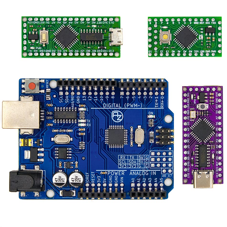
The most common are the Arduino Nano and Pro Mini compatible boards, which can be found as “LGT8F328P LQFP32 MiniEVB” in online stores for a few Euros. The Arduino UNO compatible board I tested is from AZ-Delivery. It is a bit different from the other boards in some aspects.
The LGT8F238P IC is available as an SSOP version with 20 pins (SSOP20), as QFP with 48 pins (QFP48L) or as QFP with 32 pins (QFP32L). In this article, I only deal with QFP32L based boards, which are closest to the ATmega328P based representatives. Mostly, they are labeled with “LQFP32”. I will discuss all three versions in a follow-up article. They have the same registers and essentially only differ in which functions are actually accessible through pins.
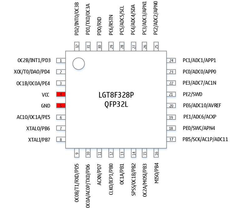
The pinout scheme of the QFP32L shows many similarities to that of the ATmega328P, but also a few additional features.
A certain disadvantage when working with the LGT8F328P is that the manufacturer does not provide an English data sheet. However, thanks to some hardworking contributors, translations are available, for example here on GitHub.
Advantages compared to the ATmega328P
I don’t want to list here all the technical features of the LGT8F328P. Like the ATmega328P it has 2 KB SRAM, 32 KB flash, the supply voltage is from 1.8 to 5.5 volts etc.
These are some important differences to the ATmega328P:

Pinout of the LGT8F328P-LQFP32 based boards
When comparing the LGT8F328P boards with their ATmega328P counterparts, you have to look twice to see differences. This applies in particular to the pin labels. Here you can see an original Arduino Nano (blue), next to two LGT8F328P Nano boards:

There are also great similarities with the originals in terms of pin functions:
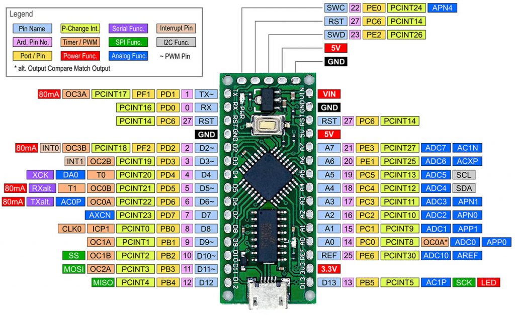
A corresponding diagram for the LGT8F328P based Pro Mini can be found here, for example. For UNO-like board I tested (source: AZ-Delivery) I did not find such a scheme. But this should not be a problem because the UNO has the same in- and outputs. Only SWC and SWD are missing.
Installation of the board package
Nano- / Pro Mini-like boards
To be able to program the LGT8F328P boards with the Arduino IDE, you must first install a suitable board package. For the “L-Nano” (as an abbreviation for “LGT8F328P based”) and the “L-Pro Mini” I used the great board package lgt8fx from David Buezas. It is based on the packages Larduino_HSP and LGT but is easier to handle, takes better advantage of the LGT8F328P and is better documented. You can learn more about the differences here.
A detailed installation guide for the board package with screenshots can be found here. The short version is:
- Go to File → Preferences.
- Click the button behind “Additional Board Manager URLs”.
- Enter there the line “https://raw.githubusercontent.com/dbuezas/lgt8fx/master/package_lgt8fx_index.json” (without quotes).
- Navigate to Tools → Board: “xxx” → Boards Manager.
- Search for “lgt8fx” and install the package “LGT8fx Boards” by dbuezas.
After successful installation, select “LGT8F328” as the board. As “Variant” I have selected “328P-LQFP32 (e.g. MiniEVB nano-style or WAVGAT)”.

UNO-like board
For AZ-Delivery’s UNO-like board, the procedure is similar. The entry for the board manager URL is:
- http://www.az-arduino.de/package_AZ-Boards_index.json
In the board manager menu, search for “AZ boards”. You can find a detailed description in the free e-book from AZ-Delivery.
Checking the installation
Take any sketch, for example Blink.ino from the “Basics” example sketches of the Arduino IDE and upload it. The board LED should flash every second.
How to upload sketches via an USB-to-TTL adapter (e.g. for the Pro Mini) or via LGTISP and how to burn the bootloader, I explain at the end of the article (here).
LGT8F328P-LQFP32 boards in action
Enough of the preparations and general explanations – now we come to the more interesting, practical part.
I have tried many Arduino sketches with all kinds of functions unchanged on the LGT8F328P boards. Only sketches that use the watchdog timer and sleep functions had to be adapted. Everything else worked 1:1. So we can essentially focus on the additional functions.
Analog to digital converter
You can read the voltage at an analog pin via analogRead() as you are used to from the ATmega328P based boards. The default resolution is 10 bit. The standard reference voltage is the operating voltage (VCC).
It should be noted that the “Nano-like” board has a diode built into the 5 volt line to protect the USB port. The effective operating voltage is therefore about 4.6 volts when powered via USB. You can find the diode above the pins D10 / D11.
As with the conventional ATmega328P boards, you can use external voltage references. If you do this, connect it to the REF input. Alternatively, the LGT8F328P provides internal references of 1.024, 2.048 or 4.096 volts. Furthermore, the LGT8F328P allows you to increase the resolution to 11 or 12 bits. The following sketch shows how it works:
/*
    Parameter:      Reference:
    DEFAULT         VCC
    EXTERNAL        External Reference (REF)
    INTERNAL1V024   Internal 1.024 volts
    INTERNAL2V048   Internal 2.048 volts
    INTERNAL4V096   Internal 4.096 volts
*/

void setup(){
    Serial.begin(9600);
    analogReference(INTERNAL4V096);
    analogReadResolution(10); // Resolution = 10, 11 or 12 Bit
}
void loop(){
    int adcValue = analogRead(A1);  // Raw value
    float voltage = adcValue * 4.096/1024.0;  // Voltage calculation
    Serial.print("Analog Value: ");
    Serial.println(adcValue);
    Serial.print("Voltage [V]: ");
    Serial.println(voltage,3);
    delay(1000);
}
AD converter quality
The good news: The LGT8F328P’s ADC works quite linearly. The bad news is that the noise is at least as high as with the AVR-based boards. Even in the 10-bit resolution, I had to average at least 100 readings to get stable values. Unfortunately, this makes an 11- or 12-bit resolution of limited use! Maybe the noise can be reduced by stabilizing the supply voltage – I have to experiment a bit more.
Let’s focus on the positive. I tested the ADC by applying voltages with my lab power supply and converting them with the LGT8F328P. I checked the voltages with a reliable multimeter. The internal 4,096-volt reference was used for A/D conversion, and 100 readings were averaged for each data point. I did the test with different several boards. This is a typical result:
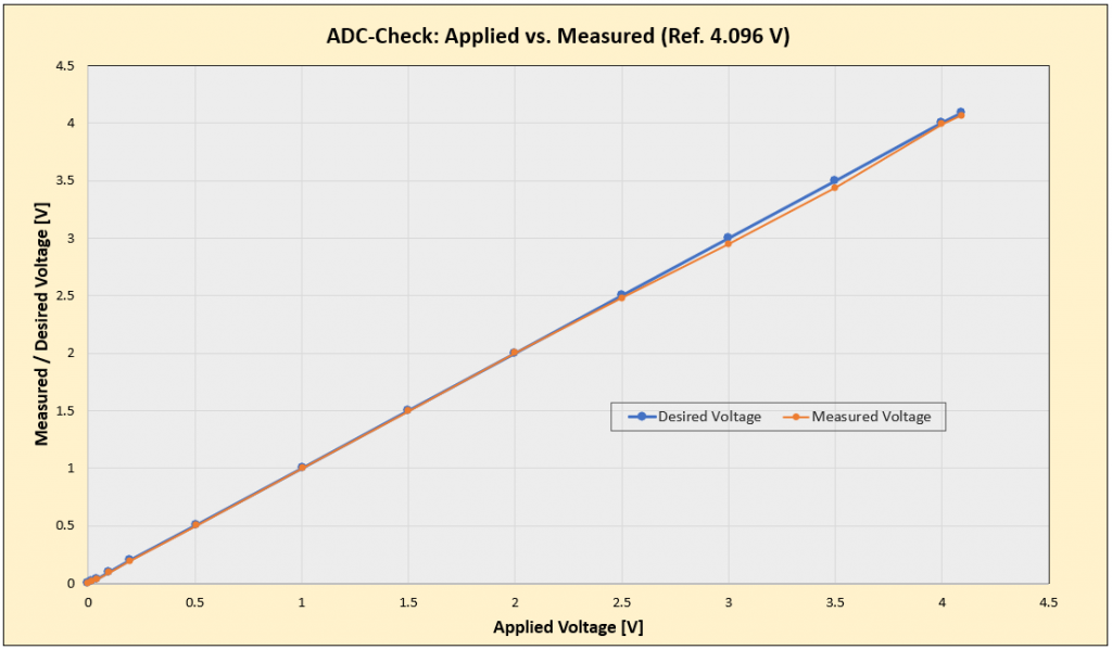
Each board had an individual, small and reproducible deviation. So if you need very accurate results, you can use Excel or similar programs to create a best-fit curve.
Analog differential measurements and gain
The LGT8F328P allows you to perform differential measurements between specific analog inputs. You can amplify the differential voltages by a factor of 1, 8, 16 or 32. The function for this is analogDiffRead(). It expects the negative input, the positive input and the gain factor as arguments. To use the function, you have to include the differential_amplifier.h library file.
Here is an example sketch:
#include<differential_amplifier.h>
/*
    Parameter:      Reference:
    DEFAULT         VCC
    EXTERNAL        External Reference (REF)
    INTERNAL1V024   Internal 1.024 volts
    INTERNAL2V048   Internal 2.048 volts
    INTERNAL4V096   Internal 4.096 volts

 Available combinations:
| -\+ | A0  | A1  | A2  | A3  | A4  | A5  | A6  | A7  |
| --- | --- | --- | --- | --- | --- | --- | --- | --- |
| A0  |     |  +  |     |     |     |     |     |     |
| A1  |  +  |     |     |     |     |     |     |     |
| A2  |  +  |  +  |     |  +  |  +  |  +  |  +  |  +  |
| A3  |  +  |  +  |  +  |     |  +  |  +  |  +  |  +  |
| A4  |  +  |  +  |     |     |     |     |     |     |
| A5  |  +  |  +  |     |     |     |     |     |     |
| A6  |  +  |  +  |     |     |     |     |     |     |
| A7  |  +  |  +  |     |     |     |     |     |     |
*/

void setup(){
    Serial.begin(9600);
    analogReference(INTERNAL4V096);
}
void loop(){
    int raw = analogDiffRead(A2,A3,GAIN_16); // GAIN_x mit x = 1, 8, 16, 32
    float voltage = raw / 1024.0 * 4096.0 / 16.0; // considers resolution, reference and gain
    Serial.println(voltage);
    delay(1000);
}
As you can see from the table in the sketch, only certain combinations of analog inputs are allowed for differential measurements. If you choose an invalid combination, you will get a raw value of -1.
To use differential_amplifier.h with AZ-Delivery’s LGT8F328P based UNO, the easiest way is to download the lgt8fx package from here and extract the corresponding “.cpp” and “h.” files from the lgt8f/libraries/differential_amplifier folder and save them to the sketch’s folder. In this case, the header file in #include needs to be put in quotation marks.
Digital to analog converter
“Quasi-analog” PWM signals
As known from the ATmega328P boards, you can tap a PWM signal at (Arduino) pins 3, 5, 6, 9, 10 and 11 with analogWrite(). Likewise, the PWM frequency on pins 5 and 6 is twice as high as on the other pins. It should be noted that the frequencies depend on the clock rate. At 16 MHz they correspond to those of the ATmega328P boards, namely 490 and 980 Hertz respectively. The frequency changes proportionally with the clock rate.
I will explain how to generate PWM signals at pins 1 (TX) and 2 (D2) when we get to the timers. Some pinout schemes found on the net additionally mark pin 8 as PWM pin. However, this is wrong.
Generating a real analog signal
At pin 4 (D4 / PD4 / DAO) you can generate a real analog signal with a resolution of 8 bit. By default, VCC is the reference, i.e. 255 ≙ VCC. Alternatively, you can use an external reference or the internal references 1,024, 2,048 or 4,096 volts. The following little sketch shows how it works:
/*
    Parameter:      Reference:
    DEFAULT         VCC
    EXTERNAL        External Reference (REF)
    INTERNAL1V024   Internal 1.024 volts
    INTERNAL2V048   Internal 2.048 volts
    INTERNAL4V096   Internal 4.096 volts
*/

void setup(){
    analogReference(DEFAULT);
    pinMode(DAC0, ANALOG);
    analogWrite(DAC0, 125); // 0...255
}
void loop(){}
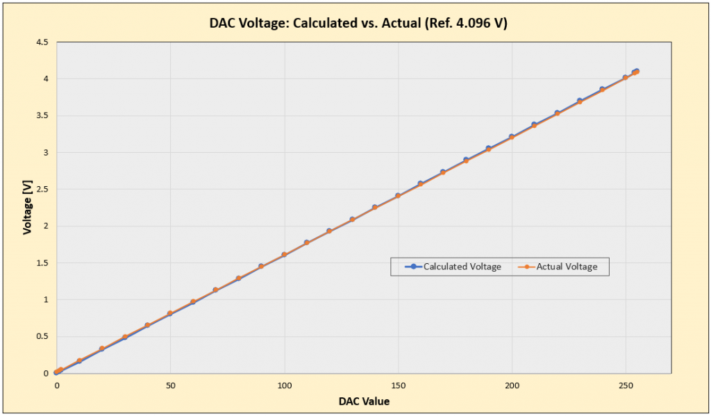
Accuracy of the DAC
I checked the accuracy of the analog signal with the 4.096 volt reference and was quite impressed with the correlation between the calculated and measured value:
Using the 80 mA outputs
Because of the ambiguity of the different pin designations (e.g. 1 vs. TX vs. PD1 vs. D1), I use the labels on the LGT8F328P Nano board in the following when referring to the board pins.
The pins TX, D2, D5 and D6 can supply up to 80 mA. However, you must first enable this “high current” feature by setting the appropriate bits in the HDR register. Then you can – at least for the pins D5 and D6 – use the outputs with pinMode() and digitalWrite(). Here is an example:
/*
       HDR      Port/Pin     Pin Label (Nano)
       HDR0 --> PD5       --> D5
       HDR1 --> PD6       --> D6
       HDR2 --> PF1       --> TX
       HDR3 --> PF2       --> D2
       HDR4 --> PE4 / PF4 --> none
       HDR5 --> PE5 / PF5 --> none
*/

void setup(){
    HDR |= (1<<HDR0); // Activate high current for Pin 5
    pinMode(5,OUTPUT);
    digitalWrite(5, HIGH);
}

void loop(){}
If you want to enable the 80 mA option on pins TX and D2, there is a small complication. PD1 and PF1 share TX, PD2 and PF2 share D2 (which makes naming the pins uniquely even more difficult). However, the high current option is only provided via PF1 and PF2 and not via PD1 or PD2. But since PF1 and PF2 are not implemented as Arduino pins (on the QFP32L), you have to address them directly via the ports. Here is a “high current blink sketch” for PF2:
/*
       HDR     Port/Pin      Pin Label (Nano)
       HDR0 --> PD5       --> D5
       HDR1 --> PD6       --> D6
       HDR2 --> PF1       --> TX
       HDR3 --> PF2       --> D2
       HDR4 --> PE4 / PF4 --> none
       HDR5 --> PE5 / PF5 --> none
*/


void setup(){
/* example for activating PF2 for high current */
    HDR |= (1<<HDR3);
    DDRF = (1<<PF2);  // ~ pinMode OUTPUT
}

void loop(){
    PORTF |= (1<<PF2); // Pin HIGH
    delay(1000);
    PORTF &= ~(1<<PF2); // Pin LOW
    delay(1000);
}
But here you have to be careful: If PF1 or PF2 are in OUTPUT / HIGH state and PD1 or PD2 are in OUTPUT / LOW state you could cause a short circuit (I didn’t try it). And PD1 could be accidentally set to this state by its TX function.
If you are not familiar with bit operations and port manipulations such as PORTF &= ~(1<<PF2), I recommend reading my post on this topic.
Watchdog Timer (WDT)
Maybe one or the other has read my post about the watchdog timer of the ATmega328P. The sketches I published there, work only to a limited extent on the LGT8F328P boards. If you want to use the WDT, it is best to use the library WDT included in the board package lgt8fx (instead of avr/wdt.h). Here is an example sketch:
/*
    Parameter   WDT Reset Period
    WTO_64MS         64 ms
    WTO_128MS       128 ms
    WTO_256MS       256 ms
    WTO_512MS       512 ms
    WTO_1S            1 s
    WTO_2S            2 s
    WTO_4S            4 s
    WTO_8S            8 s
    WTO_16S          16 s
    WTO_32S          32 s
*/

#include <WDT.h>

void setup() {
    Serial.begin(9600);
    Serial.println("Sketch started");
    wdt_enable(WTO_8S);
}

void loop() {
    for(int i=0; i<1000; i++){
        Serial.print("Runtime [s]: ");
        Serial.println(i);
        delay(1000);
//        wdt_reset();
    }
}
A restart is triggered after every eight seconds. However, if you uncomment line 28, the sketch will run forever.
WDT Interrupt
To use the WDT ISR, take the function wdt_ienable(). Here is an example:
#include <WDT.h>

volatile boolean isrflag;

void setup() {
    pinMode(LED_BUILTIN, OUTPUT);
    digitalWrite(LED_BUILTIN, LOW);
    Serial.begin(9600);
    Serial.println("Sketch started.");
    isrflag = false;
    wdt_ienable(WTO_4S);
}

void loop() {
    int n = 0;
    do {
        Serial.print("Elapsed time: ");
        Serial.print(n);
        Serial.println(" s");
        delay(1000);
        if (digitalRead(LED_BUILTIN))
            digitalWrite(LED_BUILTIN, LOW );
        else
            digitalWrite(LED_BUILTIN, HIGH);
        if (isrflag) {
            Serial.println("--There was a wdt interrupt.--");
            isrflag = false;
            wdt_enable(WTO_4S); // uncomment this line...
            // wdt_ienable(WTO_4S);   // ...comment this line and see the change
        }
        // wdt_reset(); // if uncommented, no interrupt will occur
    } while( n++ < 1000 );
}

ISR (WDT_vect)
{
    isrflag = true;
    wdt_reset();
}
If you don’t want to reset the LGT8F328P after the interrupt, then change lines 28 and 29 from wdt_enable() to wdt_ienable().
Sleep and power modes
If you want to put your LGT8F328P board into sleep mode, it is best to use the PMU library included in the board package.
To try out the following example sketch, connect pin 2 (D2) to GND via a push button. With the settings selected in the sketch, your board will be sent to sleep, wake up after four seconds, then be sent to sleep again, and so on. If you press the push button, your board wakes up immediately due to the external interrupt.
/*
    Power Modes
    PM_IDLE0:     disable core clock only
    PM_POWERDOWN: disable most clocks and switch main clock to rc32k
    PM_POFFS0:    power off all core functions (digital and analog)
                  wake up by external interrupt or periodly
    PM_POFFS1:    the lowest power mode which close all modules and clocks
                  wake up by external interrupt only

    Sleep Duration:
    SLEEP_xMS with x = 64, 128, 256, 512 (milliseconds), e.g. SLEEP_256MS
    SLEEP_yS  with y = 1, 2, 4, 8, 16, 32 (seconds), e.g. SLEEP_4S
    SLEEP_FOREVER
*/

#include <PMU.h>
const int interruptPin = 2;

void setup(){
    Serial.begin(9600);
    Serial.println("Sketch started!");
    pinMode(interruptPin, INPUT);
    digitalWrite(interruptPin, HIGH);
    attachInterrupt(digitalPinToInterrupt(interruptPin), noAction, FALLING);
}

void loop(){
    Serial.flush();
    PMU.sleep(PM_POWERDOWN, SLEEP_4S);
    Serial.println("Woke Up!");
    delay(200); // for debouncing
}

void noAction(){} // dummy
Fastio – Functions
The functions pinMode(), digitalWrite() and digitalRead() have a lot of ballast that you don’t need in most cases. If you want to save a few microseconds, you can use port manipulation. If this is too cryptic for you, fastioMode(), fastioWrite(), fastioRead() and fastioToggle() are available as alternatives.
The disadvantage of the functions is that you cannot pass them variable names, only the pin as a number. If you try it anyway, you will get error messages.
Here is an example of correct usage:
void setup() {
    fastioMode(8, OUTPUT); // equals: DDRB |= (1<<PB0);
}

void loop() {
    fastioWrite(8, HIGH); // equals (in essence): PORTB |= (1<<PB0);
    delay(100);
    fastioWrite(8, LOW);  // equals (in essence): PORTB &= ~(1<<PB0);
    delay(100);
    fastioToggle(8); // equals: PINB = (1 << PB0);
    delay(1000);
    fastioToggle(8); // equals: PINB = (1 << PB0);
    delay(1000);
}
Using fastioRead() is just as easy:
int status = fastioRead(8); // equals: int status = (PINB >> PB0) & 1;
The fastio functions are not a special feature of the LGT8F328P, but just a nice feature of the board package.
Timer and PWM
The LGT8F328P has two 8-bit and two 16-bit timers, so one 16-bit timer more (Timer3) than the ATmega328P. Timers 0 to 2 include two output compare registers each, which you can use to generate PWM signals at the assigned outputs OCxA/OCxB. I have explained how this works in my posts about Timer0 and Timer1 and about Timer2. All sketches used there also work on the LGT8F328P.
Three output compare registers and the three outputs OC3A, OC3B and OC3C belong to the Timer3.
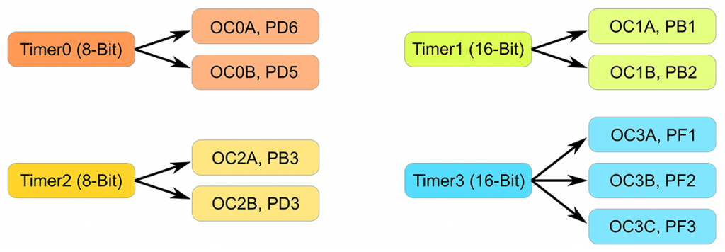
The pinout diagram of the LGT8F328P-QFP32L (see at the very top) is somewhat misleading in this regard. It is correct that OC3C has no output pin. It is also true that OC3A and OC3B are accessible at the pins for PD1 and PD2. However, to obtain a PWM signal, you have to set PF1 and PF2 to OUTPUT. PF1 and PF2 share their outputs with PD1 and PD2, as already mentioned.
Here is an example of a fast PWM signal at PF1 (board pin: TX) with a duty cycle of 25% and a frequency of 2 kHz (when the LGT8F328P is running at 32 MHz):
void setup(){
  // Clear OC3A on Compare Match / Set OC3A at Bottom; Wave Form Generator: Fast PWM 14, Top = ICR3
  TCCR3A = (1<<COM3A1) + (1<<WGM31);
  TCCR3B = (1<<WGM33) + (1<<WGM32) + (1<<CS30); // prescaler = 1;
  ICR3 = 15999;
  OCR3A = 3999;
  DDRF |= (1<<PF1);
}

void loop() {}
Further explanations would lead too far here – if you are interested, have a look at the already mentioned articles about the timers of the ATmega328P. Or, if you don’t feel like calculating and picking all the bits out of the tables, you might want to try this great tool by David Buezas:Arduino Web Timers. You find the documentation here on GitHub.
By the way, you can set the Timer0 and Timer1 counter to double the system frequency, i.e. up to 64 MHz! For this, you have to set the F2XEN bit in the “Timer Counter Clock Control and Status Register” (TCKCSR). By setting the bits TC2XS0 for Timer0 or TC2XS1 for Timer1 you tell the LGT8F328P which timer should run at double speed. E.g.:
TCKCSR = (1 << F2XEN) | (1 << TC2XS0);
One more reason to use David Buezas’ tool.
Programming the LGT8F328P based Pro Mini
Upload via USB-to-TTL adapter
The counterpart to the Arduino Pro Mini (“L-Pro Mini”) lacks, just like the original, the on-board USB-to-TTL adapter. So, you need to attach one as an external module. Programming is most convenient if you take an adapter which has a DTR pin.


The adapter shown here also has the advantage that you can plug it directly onto the “L-Pro Mini”, as long as you have soldered on a pin header beforehand.
If you connect everything by cable, you have to make sure that you connect RX to TX and TX to RX.
Uploading is simple: select the port your adapter is connected to, and then simply upload.
If you have a USB-to-TTL adapter without a DTR pin, it’s a little bit more complicated. When you initiate the upload process, press the reset button of the board you want to program. Release the button when the compilation is completed and the actual upload should start.
Upload via LArduinoISP (without bootloader)
As we have already seen, the LGT8F328P has significant differences “under the hood” despite all compatibility with the ATmega328P. This is also shown by the fact that it is not programmable via its pins 11, 12 and 13 by ISP. Instead, it has two pins, SWC and SWD, for this purpose.
But as with the ATmega328P, you can also convert a LGT8F328P based board to an ISP programmer.
For the “LGT8F328P – UNO” from AZ-Delivery this makes little sense because this board does not have the SWC and SWD pin accessible.
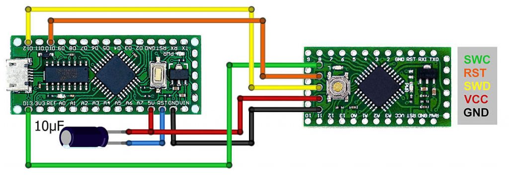
Turning an LGT8F328P board into a programmer
Connect the LGT8F328P based board that will serve as a programmer to your computer. It is best not to connect anything else to the board. Then you perform the following steps:
- Select the connected board in the Arduino IDE.
- Under Tools → “Arduino as ISP” you set the option “[To burn an ISP] SERIAL_RX_BUFFER_SIZE to 250” (see below, blue selection).
- Go to File → Examples → “Examples for LGT8F328” in the menu and select the sketch LarduinoISP.
- Upload the sketch.
- Set “Arduino as ISP” in Tools back to default (64).

The programmer is ready!
Uploading sketches
Connect your new programming device to the board to be programmed (“target”) as follows:
| Programmer | Target |
| GND | GND |
| 5V | VCC |
| Pin 12 (D12) |
SWD |
| Pin 10 (D10) |
RST |
| Pin 13 (D13) |
SWC |
To prevent a reset of the programmer when uploading to the target, connect the RST pin of the programmer via a 10 µF capacitor to the 5 V pin. If you don’t have a capacitor, you can connect the two pins directly, but then you must not press the reset button of the programmer (short circuit!).
This is how the setup looks, for example, with an “L-Nano” as the programming device and an “L-Pro Mini” as the target device:
Choose the following settings in the Arduino IDE:
- Select the target as board.
- Under Tools → Programmer you set “AVR ISP”.
To upload, choose Sketch → Upload with Programmer or use the key combination: Ctrl + Shift + U.
Bring back the bootloader
If you upload a sketch via LarduinoISP, the bootloader will be deleted. To program the board again directly via USB or USB-to-TTL adapter, you have to burn the bootloader first. Nothing easier than that: Use the same settings as when uploading via LarduinoISP and click on Tools → Burn Bootloader.
Problems with the purple LQFP32 board as LArduinoISP programmer
The purple LQFP32 board with the CH9340C USB-to-TTL chip cannot be used as a LArduinoISP programmer for reasons unknown to me so far.
Conclusion
LGT8F328P based boards are a high-performance alternative to their ATmega328P counterparts. Thanks to the available board packages, the LGT8F328P boards are easy to handle. Sketches you have written for ATmega328P boards can be used in most cases without any changes. The LGT8F328P offers some additional, useful features.
Acknowledgement
I’d like to thank David Buezas, LaZsolt and dwillmore for the excellent work on the board package lgt8fx and for the review of this article.
hi Sir
i have purchased some Atmega328p which I couldn’t program
& even checked for hardware connections & no GND connection between pin3 $ pin21
someone suggested to try the lgt
im looking for programming the ltg8f328p chip using Arduino Uno for example
is that ok ?
thanks
Hi,
if your ATmega328P chips don’t work, maybe you should try buying them from a more reliable source? But of course you can also try using an LGT8F328P which has some advantages. Programming via an Arduino UNO is possible, however I have not tried this. You find a library including instructions here: https://github.com/SuperUserNameMan/LGTISP
But it’s much easier if you use another lgt8f328p board for this purpose.
Good luck!
Sir please put some tutorial lessons on Nuvaton microcontroller . as its cheaper than all 8bit micros availble in market.
Hi, thanks for the proposal. I will have a deeper look into this myself first.
One important warning especially about the pro mini style boards.
Those DO NOT have an external crystal. Which results in broken I2C communication!! The internal clock isn’t stable enough. Those who not believe me may try themselves.
I had to switch to a nano style, luckily i had one with a crystal. The green version seems not to have a crystal, at least not on the top. Be careful!
No I2C means you can not use I2C displays, tons of modules and sensors, or repurpose it as I2C DAC. That makes the pro mini very limited in possible applications. Don’t know about SPI.
About the boards with crystal i can’t complain so far. I like the boards for the DAC.
Hi, thanks for sharing your experience. I have not not faced such I2C issues yet when using the Pro Mini style boards. I hope I find some time soon to test some of my boards with some I2C devices more intensively.
I had this bad surprise with 0,96″ I2C OLED displays.
For short periods it sometimes works, but at the end it always breaks. This doesn’t happen when the board has a crystal.
Thanks, will try it. But will take a bit. I want to complete something else first.
Hi, finally I found the time to test a display. I used an 0,96″ I2C OLED display (SSD1306 controller). I wrote a little sketch that just displays the elapsed time since the sketch has started. It has been running for more than two hours as you can see on the photo. Maybe you got a bad quality Pro Mini style board?
So at least I wouldn’t say that this is a general issue of these boards.
Regards, Wolfgang
Thanks for going so far to test out the board for us. Your article has been super duper helpful.
Du bist the GOAT!
Thank you 🙂 !
Hi there! Thanks for this article. Does that mean it still can’t be used as a ISP programmer? Say for example I want to program ATtiny85 via this? I could easily get the ATtiny85 with the ports for direct programming, but just getting the IC seems cheaper, and I already have the LGT8F328P on the way to try out.
Hi, as far as I can see, the issue that was raised omn GitHub is still open:
https://github.com/dbuezas/lgt8fx/issues/312
However, I would try it. Firstly, I have not tried this board as an ISP Programmer for AVR microcontroller, secondly maybe you get a different version or different production batch that works better. You never know with these devices from China. It would be great if you share your experience after trying. Good luck!
Updated URL for the manufacturer’s page on their AVR clone (?) lineup: http://www.prodesign.com.cn/8bit-general-mcu/
thank a lot ……………very very good explanation !!
!!!!!!!!!!!!!!!!!!!!!!!!!!!!!!!!!!!!!!!!!!!!!!!!!!!!!!!!!!!!!!!!!!!wonderful
Questo è di gran lunga il miglior articolo sul chip lgt328p. 👏
Grazie per la tua ricerca e per il tuo contributo alla comunità Android Core per questo chip,
!!!!!!!!!!!!!!!!!!!!!!!!!!!!!!!!!!!!!!!!!!!!!!!!!!!!!!!!!!!!!!!!!!!wonderful
Thank you so much for this amazingly detailed information. You must have put so much time and effort in. I’m grateful for this as I am finding my way, self learning the world of micro controllers, electronics and coding. Late to the party (56) but hoping this’ll be my plan for keeping self sane in retirement!
Is it possible to extend the available space for the code? I see eeprom mentioned and wonder if this is accessible? If so how?
Thank you for your time.
Thank you for your kind feedback. It’s really quite time-consuming. Therefore, my family does not like my hobby!
The LGT8F328P emulates the EEPROM and uses ~2kb of flash for it. I don’t know a way to use this space as flash. It would be great to have a setting in the IDE deactivating the EEPROM emulation.
So perhaps utilising PROGMEM where possible saves SRAM space. Does PROGMEM utilise EEPROM space? Are there other ways of limiting SRAM space or being efficient with code?
Apologies if this is more a coding question rather that electronics type of question. Thanks for your time 🙏
PROGMEM does not use EEPROM space. But both can be used to save SRAM. For the LGT8F328P one might consider using the EEPROM instead of PROGMEM in case Flash is short. Other options to save SRAM are:
Thank you for the advice 🙏🏼
Hi there,
Excellent page. I have just one question – on the SSOP20 version using internal oscillator, are pins PB6, PB7 and PE0 and PE2 usable as I/O?
Hi,
thanks! PE0/PE2 can be used as I/O. But then, next time you upload another sketch, you need to press the reset button right before the upload.
PB6/PB7 can be used as I/O pins in theory, but the IC pins are not connected to a board pin. If you are skilled in fine soldering you could directly connect to the IC pins.
In the following article I describe the different boards and their pinouts in detail.
https://wolles-elektronikkiste.de/en/minievb-boards-an-overview
Regards, Wolfgang
Hi again! I just double checked, and the timer code is fine! It’s the usual case of having one too many things on the bench and not having enough cable! All your examples and my code run just fine!
Thanks again for the great write-ups!
Hi, great that you could solve the problem. And thanks for the feedback!
Cheers, Wolfgang
Hi Wolfgang and thanks, as always, for the very thorough and enlightening review. I have one of the purple boards and ‘basic tests’ as well as (for instance) encoder reading, ADC from a sketch for the nano work fine. However, none of the timer code does. You had mentioned that your timer examples ‘just work’ but I couldn’t verify. This is the code which works on a 328p (nano):
// PWMPIN = 11
pinMode(PWMPIN, OUTPUT);
ASSR &= ~(_BV(EXCLK) | _BV(AS2));
TCCR2A |= _BV(WGM21) | _BV(WGM20);
TCCR2B &= ~_BV(WGM22);
// Do non-inverting PWM on pin OC2A (p.155)
// On the Arduino this is pin 11.
TCCR2A = (TCCR2A | _BV(COM2A1)) & ~_BV(COM2A0);
TCCR2A &= ~(_BV(COM2B1) | _BV(COM2B0));
// No prescaler (p.158)
TCCR2B = (TCCR2B & ~(_BV(CS12) | _BV(CS11))) | _BV(CS10);
// Set initial pulse width to the first sample.
OCR2A = 0;
// Set up Timer 1 to send a sample every interrupt.
cli();
// Set CTC mode (Clear Timer on Compare Match) (p.133)
// Have to set OCR1A *after*, otherwise it gets reset to 0!
TCCR1B = (TCCR1B & ~_BV(WGM13)) | _BV(WGM12);
TCCR1A = TCCR1A & ~(_BV(WGM11) | _BV(WGM10));
// No prescaler (p.134)
TCCR1B = (TCCR1B & ~(_BV(CS12) | _BV(CS11))) | _BV(CS10);
// Set the compare register (OCR1A).
// OCR1A is a 16-bit register, so we have to do this with
// interrupts disabled to be safe.
OCR1A = F_CPU / SAMPLE_RATE; // 16e6 / 8000 = 2000
// Enable interrupt when TCNT1 == OCR1A (p.136)
TIMSK1 |= _BV(OCIE1A);
sei();
Do you see anything that might trip up? I thought of the workaround for OCR1A, perhaps?
HI Wolfgang,
MANY THANKS FOR YOUR ARTICLE! IT’S GREAT. I WOULD LIKE TO ASK YOU FOR A LITTLE CLARIFICATION.
WHEN I TRY TO TURN ON THE HIGH CURRENT FOR PIN 5, THE COMPILER TELLS ME THAT HDR IS NOT DECLARED.
/*
HDR Port/Pin Pin Label (Nano)
HDR0 –> PD5 –> D5
HDR1 –> PD6 –> D6
HDR2 –> PF1 –> TX
HDR3 –> PF2 –> D2
HDR4 –> PE4 / PF4 –> none
HDR5 –> PE5 / PF5 –> none
*/
void setup(){
HDR |= (1<<HDR0); // Activate high current for Pin 5
pinMode(5,OUTPUT);
digitalWrite(5, HIGH);
}
void loop(){}
DO I NEED TO INCLUDE ANY LIBRARIES? THANK YOU VERY MUCH
Hi, the sketch in my article worked as is. So, as long the makers of the Board package have not changed anything it should work without inclding libraries. But of course the lgt8fx board package needs to be installed. Have you done this? And which board have you chosen in the Arduino IDE?
Hi, thanks for your so quick response! I have been using the LGT board for almost 6 months, I have already used it for several projects. But maybe I didn’t use the Buezas package as you describe in the article, I no longer remember which one I loaded. Maybe that’s the problem!
Incredible article, thank you so much!
Thanks for your kind feedback!
Dear Wolfgang;
It seems have alternative USART pins RX TX at D5 D6 but i could not find any documentation how to use. May be just refered as Serial1 ? Do you have tested ??
Hi Antonio, I have described how to use alternative pins here:
https://wolles-elektronikkiste.de/en/minievb-boards-an-overview#using_alternative_pins
I have tried it for reallocation of PWM pins, bit it should work for the serial pins in the same way. Still, there is only one serial connection. If you need more, then you could use SoftwareSerial.
Ok . Thanks for informations.
Hi Wolfgang,
thanks a lot for your write-up, it helps a lot!
A short question
I have the purple “nano” board with USB-C, the one in the lower left on your photo. It comes with two LEDs onboard, a blue one on the USB side, and a red one at the other end.
Do you know if (and if so, how) I can access both of them? LED_BUILTIN from the famous Blink Example seems to only blink the blue one…
Greetings,
Andreas
Hi Andreas, the red LED is connected to the VCC pin of the LGT8F32P. Therefore it is on as long as the board is powered, regardless of whether the power is supplied via USB, 5V, 3.3V or VIN. So, no chance to control the LED via sketches. But you can remove it if it bothers you. Regards, Wolfgang
Thanks a lot & Greetings from Berlin 🙂
And if anyone noticed… the purple board is on the lower right, not left, sorry for the confusion 🙂
Hi, I didn’t check but I am almost 100% certain fastioToggle(8); does NOT equal to PORTB ^= (1<<PB0); because that results in three assembly instructions (read, modify, write e.g. IN, EOR, OUT). The way to toggle the output on AVRs is to write to PINx register which is INPUT register but writing to it (which is only one assembly instruction e.g. OUT) causes toggling the OUTPUT. Because of that, fastioToggle(8); probably equals PINB = (1 << PB0); which is much faster because that is only one OUT instruction vs one IN instruction, plus one EOR instruction plus one OUT instruction which is the reason why writing to PINx is implemented in hardware.
Well spottet! fastioToggle(8) equals PINB = (1 <<PB0) as one can find here:
https://github.com/dbuezas/lgt8fx/blob/master/lgt8f/cores/lgt8f/fastio_digital.h
Thanks!
nice manual for arduino users, thanks a lot, i got many usefull info about this chip
Thank you!!!
This is by far the best article on the lgt328p chip 👏
Thanks for your research and your contributions to the community android core for this chip Wolfgang!
Thank you for your kind comment. This very motivating!
Do you have any idea if these devices can be programmed with
platformIO?
It seems it’s possible, but not yet straightforward. There is an ongoing discussion on that topic on GitHub. Suggest you read this:
https://github.com/dbuezas/lgt8fx/issues/15