
About the post
In my last post I explained the basics of the ESP-01 module. You will often read that this module has two GPIOs. But there are four, because you can also address TX and RX as GPIO1 and GPIO3 respectively. Nevertheless, this can become scarce for many projects. If this is the case, then it is certainly the easiest way to switch to the big brother, the ESP-12. Alternatively, e.g. if this would not be enough, one can switch to the numerous options for ESP-01 port expansion. I would like to present three of them in this post:
- I2C 16-bit I/O Expander MCP23017
- I2C 8-bit I/O Expander PCF8574
- shift register 74HC595
The first two are addressed via I2C and therefore require two GPIOs. Three GPIOs are required for the shift register.
In a separate post I will show how to “abuse” a Counter IC for port expansion.
The MCP23017
The MCP23017 is by far the most versatile of the three components. For the “normal” breadboard user, the MCP23017-E/SP version is recommended. You can get this nice IC with its 28 legs at Conrad, Reichelt and Co for about one euro.
The MCP23017 has two ports (A and B) with eight programmable in-/outputs each. It also offers extensive interrupt programming options, which I will not discuss in detail in this post. I will only make up for this in a separate post about this interesting piece of electronics.
The MCP23017 is designed for voltages between 1.8 and 5.5 volts. In standby mode, it consumes a maximum of 1 µA.
In addition to the MCP23017, there is also the MCP23016, MCP23018 and the MCP23008 available. The latter is basically the little brother of the MCP23017 with only eight in-/outputs. Like the MCP23017, the MCP23016 and the MCP23018 have sixteen in-/outputs. I wouldn’t recommend the MCP23016 because it’s more complex to use and doesn’t offer any benefits. The MCP23018, on the other hand, is not so widely used and that’s why I introduce the MCP23017 in this post. A concise summary of the differences between MCP23xxx family members can be found here.
And here you will find a data sheet for the MCP23017.
The pinout
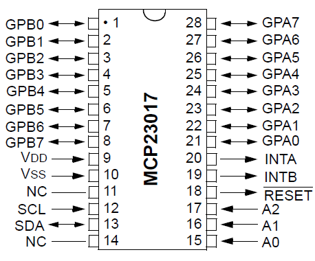
In addition to the 16 I/O pins, the Pins SDA and SCL for the I2C communication and the pins for the power supply, the MCP23017 has the following in- and outputs:
- A0, A1, A2: address pins
- RESET: low-active reset pin
- INTA, INTB: Interrupt outputs for PORT A and B; can be combined
The circuit for control by the ESP-01
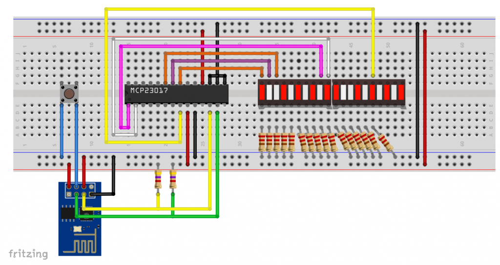
As a simple application example for the ESP-01 port extension, let’s control sixteen LEDs. In order not to make the schema too confusing, I have drawn only a small part of the lines to the LEDs. I also did not include the power supply of 3.3 volts in the circuit. I explained the upload of sketches to the ESP-01 module in my last post and therefore do not go into that detail anymore. The main aspects of the circuit are the following:
- CH_PD of the ESP-01 is hooked to 3.3 V
- Reset pin of the ESP-01 via pushbutton connected to GND
- GPIO0 to SDA
- GPIO2 to SCL
- The address pins to GND — > address is then 0x20
- the scheme is 1 0 0 A2 A1 A0
- Here: 1 0 0 0 0 0 = 32 = 0x20
- Reset pin of the MCP23017 to 3.3 V
- VSS of the MCP23017 to GND
- VDD of the MCP23017 to 3.3 V
Note: You might be tempted to power the ESP-01 module and the MCP23017 separately, especially if you are hook components to the MCP23107 that require 5 volts. The problem is that a HIGH signal to SDA/SCL must be at least at a level of 80 percent of VDD. I also fell into that trap. The error was hard to find because it didn’t fail completely, but only worked unreliable. If you want to work with different voltages, you have to put a level converter into the two communication lines.

The MCP23017 library
The MCP23017 has a lot of registers that make it very flexible, but this also makes programming a little complex. That’s why I developed a library that you can download here from Github. As already mentioned, I will publish a post about the MCP23017 at a later stage and there I will explain the library in detail. Here I limit myself to switching on and off I/O pins.
The following example sketch first creates an MCP23017 object. We don’t use the functionality of the reset. With Wire.begin(0,2);, GPIO0 and GPIO2 are defined as SDA or SCL. myMCP.Init(); defines some register contents. The function myMCP.setPinMode(); determines whether the pins act as input or output, similar to the Arduino pinMode function. With myMCP.setPort();, the HIGH/LOW states are set for an entire port. myMCP.setPin(); switches individual pins. myMCP.togglePin(); switches from HIGH to LOW or vice versa.
#define MCP_ADDRESS 0x20 // (A2/A1/A0 = LOW)
#include <Wire.h>
#include <MCP23017.h>
MCP23017 myMCP(MCP_ADDRESS,3); // 3= ResetPin, nicht weiter wichtig hier

void setup(){
  Wire.begin(0,2); //SDA = GPIO0 / SCL = GPIO2
  myMCP.Init();
  myMCP.setPortMode(B11111111,A);
  myMCP.setPortMode(B11111111,B);
  myMCP.setPort(B00000000, A); // alles auf LOW
  myMCP.setPort(B00000000, B); delay(1000);
}

void loop(){
  myMCP.setPin(1,A,ON);
  delay(1000);
  myMCP.setPin(1,B,ON);
  delay(1000);
  myMCP.setPin(1,A,OFF);
  delay(1000);
  myMCP.setPin(1,B,OFF);
  delay(1000);
  myMCP.setPort(B10101010,B00011000);
  delay(1000);
  for(int i=0; i<=7; i++){
    myMCP.togglePin(i,A);
  }
  delay(1000);
  myMCP.setPort(B00000000, A);
  myMCP.setPort(B00000000, B);
  delay(1000);
}
The PCF8574
Like the MCP23017, the PCF8574 is an I/O expander with interrupt output to be controlled via I2C. However, it has only eight in-/outputs, a single interrupt output, and does not have the many options of the MCP23017. On the other hand it is very easy to control, even without a special library or a long study of registers.
The PCF8574 is available in various versions, e.g. the DIP16 variants PCF8574P, PCF8574N or PCF8574AN. These have the same pinout differ according to my research essentially in the I2C addresses. I used the “N” variant for this post.
The PCF8574 can be operated in a range of 2.5 to 6 volts. A data sheet is available here.
A peculiarity of the PCF8574 is that the pins only provide a few hundred microamperes when in HIGH state. If you want to control LEDs, for example, you have to use the pins as input (current sink LOW). This will become clearer later in the circuit and the sketch.
The pinout

As with the MCP23017, the address is set by connecting the address pins A0, A1 and A2 to GND (0) or HIGH (1), according to the scheme “1 0 0 A2 A1 A0”. At least this applies to the variant N used by me. P0 to P7 are the inputs/outputs, INT is the low-active interrupt output and the rest should be clear.
Circuit for the control by the ESP-01
Again, I take a simple example of controlling some LEDs as an example for the ESP-01 port expansion. The fundamental difference to the MCP23017 is the current direction: it flows from the LEDs into the PCF8574 to GND. Moreover, please note:
- CH_PD of the ESP-01 is hooked to 3.3 V
- Reset pin of the ESP-01 is connected to GND via a pushbutton
- GPIO0 to SDA
- GPIO2 to SCL
- Address pins to GND — > address: 0x20
- The SDA and SCL lines need a pull-up (10 kOhm)
- If you use the interrupt output, this line also needs a pull-up
Note: also with the PCF8574, a HIGH signal must exceed a certain level in order to be recognized as such (Vmin, HIGH = 0.7 x VDD). So be aware of this if you want to use the PCF8574 with 5 volts and use a 3.3V ESP-01. You could use a level converter in this case.

A simple example sketch
First of all, one has to rethink: only when a pin is in the LOW state, current can flow according to the circuit shown above. In other words: 0 — > LED is on, 1 — > LED is off. In the example sketch I played a little with it. In the loop, all LEDs go on and off in turn. Those unfamiliar with bit operations may wonder about the line state &= ~(1<<i);. For example, if “i” is equal to 3, that means: move the 1 by 3 digits to the left (00000100), perform a bitwise negation (11111011) and execute a logical AND (11111011).
It is important to pass the pins for SDA and SCL when using the ESP-01 at Wire.begin().
Even if there is no Read in the sketch, I have integrated a read function for completeness, which queries the state of the pins. Try it out by yourselves.
#include <Wire.h>
#define PCF8574N 0x20 // Adresse, wenn A0/A1/A2 = LOW

void setup(){
  Wire.begin(0,2);
}

void loop(){
  switchPCF8574N(B11111111);
  delay(1000);
  switchPCF8574N(B10101010);
  delay(1000);
  switchPCF8574N(B01010101);
  delay(1000);
  for(int i=0; i<=7; i++){
    byte state = B11111111;
    state &= ~(1<<i);
    switchPCF8574N(state);
    delay(500);
    }
  }

void switchPCF8574N(byte datenByte){
  Wire.beginTransmission(PCF8574N);
  Wire.write(datenByte);
  Wire.endTransmission();
}

byte readPCF8574N(){
  byte data;
  Wire.requestFrom(PCF8574N,1);
  data = Wire.read();
  return data;
}
The shift register 74HC595
The shift register differs from the other two components for the ESP-01 port expansion essentially by:
- It has eight “only outputs”
- No interrupt output
- It requires three lines for control
- The microcontroller does not have to have a special bus system such as I2C or SPI
- This makes it very interesting for the ATtiny85, for example
The 74HC595 slide register is also available under different names. It doesn’t matter if you have a “74HC595”, a “M74HC595” or a “SN74HC595”. More importantly, if there is an “N” attached to it at the end, it is the DIP16 variant.
The 74HC595 can be operated in a range of 2 to 6 volts. For example, a data sheet can be found here.
The pinout

A detailed explanation of how a sliding register works would go beyond the scope of this article. I found a very good presentation here. My rough explanation: the name of the component derives from its functioning, namely that the data to be transferred is pushed bit by bit into the shift register. Each incoming bit shifts the existing one by one place (like a gun magazine that is filled with bullets – sorry for this martial comparison). From the shift register, the complete data byte is then transferred “in one go”, i.e. in parallel, to the storage register (output register).
The pins have the following functions:
- Q0…. Q7 are the outputs
- DS = data pin; the data is pushed into the shift register
- SHCP = shift register clock pin; it’s the input for the clock for pushing the data into the shift register
- STCP = storage register clock pin; it’s the input for the clock for transfer of the data into the storage register
- OE = output enable (active low); activates the outputs Q0… Q7
- MR = master reset (low active); triggers a reset
- Q7S = serial output; if more than 8 bits are pushed into the shift register, they “drop out” here
- if DS of another 74HC595 is connected here, two of these devices (or more) can be connected serially.
Circuit for the control by the ESP-01
Again, I take the simple example of an LED control. But I would also like to show you how to use two 74HC595. The main points are:
- CH_PD of the ESP-01 is attached to 3.3 V
- Reset pin of the ESP-01 is connected via pushbutton to GND
- GPIO0 is connected to SHCP of both 74HC595
- GPIO2 to STCP of both 74HC595
- GPIO1 (TX) to DS of one 74HC595
- MR to 3.3 Volt, OE to GND
- Q7S of the first 74HC595 to DS of the second 74HC595

A simple example sketch
The sample sketch shows how the control works. The state of the 16 outputs is represented as a 16-bit number (word). “0” is LOW, “1” is HIGH. With the two “shiftOut” commands, you first transfer the lower and then the upper byte of the 16-bit number. Bit operators are used again to divide the 16-bit number into two bytes. pinData&255, cuts the upper byte, pinData>>8 isolates the upper byte.
I have chosen “LSBFIRST” as parameter for the “shiftOut” command, i.e. the bitwise transmission starts with the lowest bit (LSB = least significant bit). The alternative is “MSBFIRST” (MSB = most significant bit). You can play with it if the arrangement of the LEDs should not be in the order as you want it to be. If the storage pin attached to STCP goes from LOW to HIGH, the data is transferred from the shift register to the storage register and the LEDs are switched accordingly.
int clockPin = 0; //SHCP
int storagePin = 2; //STCP
int dataPin = 1; //DS

void setup() {
  pinMode(clockPin, OUTPUT);
  pinMode(storagePin, OUTPUT);
  pinMode(dataPin, OUTPUT);
  sendOutData(0b0000000000000000);
  delay(1000);
  sendOutData(0b1110101010101010);
}

void loop() {
}

void sendOutData(word pinData){
  digitalWrite(storagePin, LOW);
  shiftOut(dataPin, clockPin, LSBFIRST, (pinData&255));
  shiftOut(dataPin, clockPin, LSBFIRST, (pinData>>8));
  digitalWrite(storagePin, HIGH);
}
Outlook
This was a small overview of the most common methods of ESP-01 port expansion. In a coming post, I will go into more detail about the MCP23017 with its many functions. And in another post on Counter ICs, I’ll come back to the port expansion again.
My intend is to use ESP8266 – 01 as WLAN controlled device (some simple integrated web GUI in it) to switch ON and OFF relays. They will be acting as switches for 220V devices and just thought that shift register with addition of opto-couplers to drive the relays will not be as bad idea, and here is your example coming handy.
Thank you so much for share that useful information!
Thanks for your feedback and all the best for your project!
This Blog focusses on Arduinos, ESP Boards and AVR MCUs using mainly the Arduino C++ language variant. Im sorry if you don’t find the MCUs or programming languages you prefer.
Hi all,
Is it an absolute necessity on the forms including this that in every code samples almost all programs are written considering an arduino (!) or similar boards even not declaring the case (board dependency) before?
It is a case that I and all others have to accept this assumption like 10 commandments!
Why not giving code samples without considering these (!) boards, what happened to all others not using them, were they all passed away?